onsemi 2N3055A
Complementary Silicon High-Power Transistor
| Part No. | 2N3055A |
|---|---|
| Datasheet | 2N3055A Download |
| Manufacturer |  onsemi |
| Description | Complementary Silicon High-Power Transistor |
| Buy | Stock & Price |
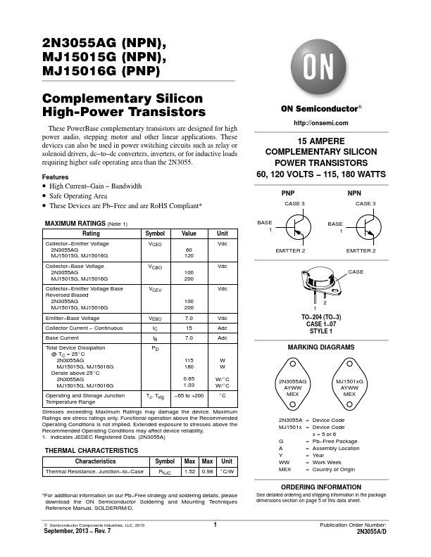
FEATURES
● High Current−Gain − Bandwidth● Safe Operating Area
● These Devices are Pb−Free and are RoHS Compliant*
MAXIMUM RATINGS
(Note 1) Rating Symbol Value Unit Collector−Emitter Voltage 2N3055AG MJ15015G, MJ15016G VCEO Vdc 60 120 Collector−Base Voltage 2N3055AG MJ15015G, MJ15016G VCBO Vdc 100 200 Collector−Emitter Voltage Base Reversed Biased 2N3055AG MJ15015G, MJ15016G VCEV Vdc 100 200 Emitter−Base Voltage Collector Current − Continuous Base Current Total Device Dissipation @ TC = 25_C 2N3055AG MJ15015G, MJ15016G Derate above 25_C 2N3055AG MJ15015G, MJ15016G VEBO 7.0 Vdc IC 15 Adc IB 7.0 Adc PD 115 W 180 W 0.65 W/_C 1.03 W/_C Operating and Storage Junction Temperature Range TJ, Tstg −65 to +200 _C Stresses exceedingMAXIMUM RATINGS
may damage the device.MAXIMUM RATINGS
are stress ratings only. Functional operation above the Recommended Operating Conditions is not implied. Extended exposure to stresses above the Recommended Operating Conditions may affect device reliability. 1. I...