onsemi 2SJ650
P-Channl Silicon MOSFET
| Part No. | 2SJ650 |
|---|---|
| Datasheet | 2SJ650 Download |
| Manufacturer |  onsemi |
| Description | P-Channl Silicon MOSFET |
| Buy | Stock & Price |
APPLICATIONS
FEATURES
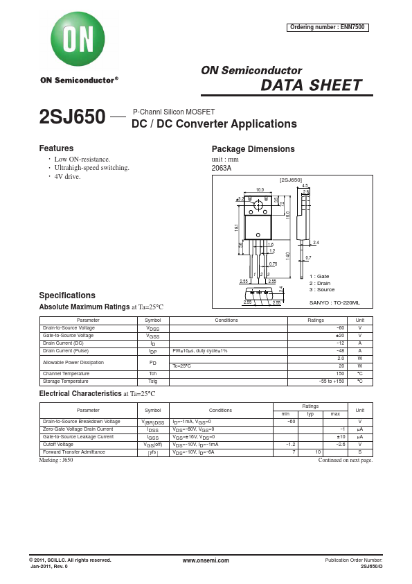
● Low ON-resistance.● Ultrahigh-speed switching.
● 4V drive. Package Dimensions unit : mm 2063A 10.0 3.2 [2SJ650] 4.5 2.8 3.5 7.2 16.0 18.1 5.6 Specifications
ABSOLUTE MAXIMUM RATINGS
at Ta=25°C 1.6 1.2 0.75 123 2.55 2.55 2.55 2.55 2.4 14.0 2.4 0.7 1 : Gate 2 : Drain 3 : Source SANYO : TO-220ML Parameter Drain-to-Source Voltage Gate-to-Source Voltage Drain Current (DC) Drain Current (Pulse) Symbol VDSS VGSS ID IDP Allowable Power Dissipation Channel Temperature Storage Temperature PD Tch TstgELECTRICAL CHARACTERISTICS
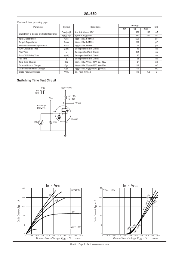
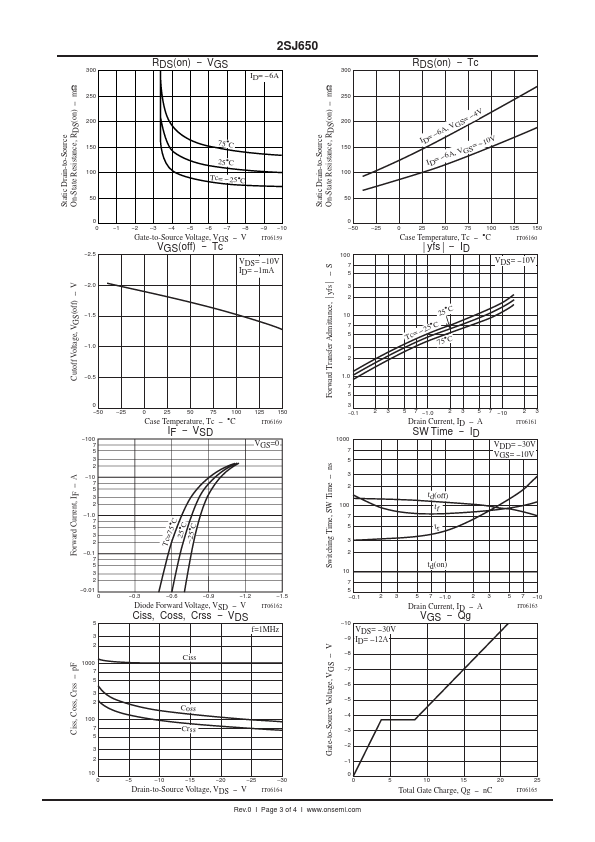
at Ta=25°C Conditions PW≤10µs, duty cycle≤1% Tc=25°C Ratings --60 ±20 --12 --48 2.0 20 150 --55 to +150 Unit V V A A W W °C °C Parameter Drain-to-Source Breakdown Voltage Zero-Gate Voltage Drain Current Gate-to-Source Leakage Current Cutoff Voltage Forward Transfer Admittance Marking : J650 Symbol Conditions V(BR)DSS IDSS IGSS VGS(off) yfs ID=--1mA, VGS=0 VDS=--60V, VGS=0 VGS=±16V, VDS=0 VDS=--10V, ID=--1mA VDS=--10V, ID=--6A min --60 --1.2 7 Ratings typ max Unit V --1 µA ±10 µA --2.6 V 10 S Continued on next page. © 2011, SCILLC.