onsemi 74HC374
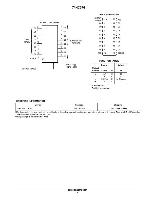
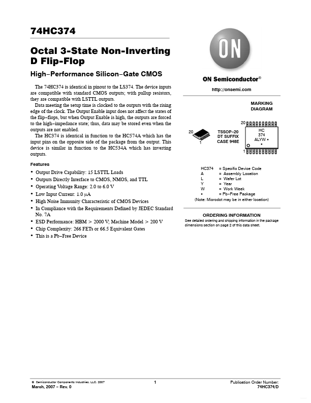
The 74HC374 is identical in pinout to the LS374. The device inputs are compatible with standard CMOS outputs; with pullup resistors, they are compatible with LSTTL outputs. The Output Enable input does not affect the states of the flip−flops, but when Output Enable is high, the outputs are forced to the high−impedance state; thus, data may be stored even when the outputs are not enabled.| Part No. | 74HC374 |
|---|---|
| Datasheet | 74HC374 Download |
| Manufacturer |  onsemi |
| Description | Octal 3-State Non-Inverting D Flip-Flop |
| Buy | Stock & Price |
FEATURES
MARKING DIAGRAM 20 20 1 TSSOP−20 DT SUFFIX CASE 948E 1 HC 374 ALYW G G●
●
●
●
●
●
●
●
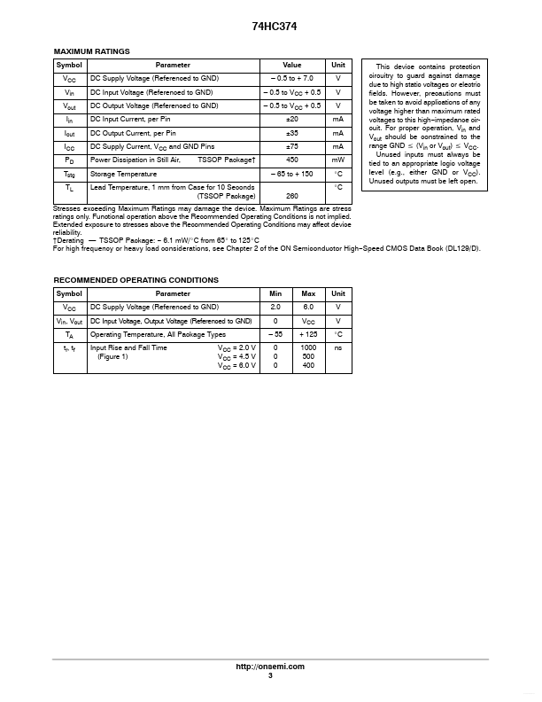
● Output Drive Capability: 15 LSTTL Loads Outputs Directly Interface to CMOS, NMOS, and TTL Operating Voltage Range: 2.0 to 6.0 V Low Input Current: 1.0 mA High Noise Immunity Characteristic of CMOS Devices In Compliance with the Requirements Defined by JEDEC Standard No. 7A ESD Performance: HBM > 2000 V; Machine Model > 200 V Chip Complexity: 266 FETs or 66.5 Equivalent Gates This is a Pb−Free Device HC374 = Specific Device Code A = Assembly Location L = Wafer Lot Y = Year W = Work Week G = Pb−Free Package (Note: Microdot may be in either location) ORDERING INFORMATION See detailed ordering and shipping information in the package dimensions section on page 2 of this data sheet. © Semiconductor Components Industries, LLC, 2007 March, 2007 − Rev. 0 1 Publication Order Number: 74HC374/D 74HC374 PIN ASSIGNMENT LOGIC DIAGRAM D0 D1 D2 DATA INPUTS D3 D4 D5 D6 D7 CLOCK 3 4 7 8 13 14 17 18 11 2 5 6...