DESCRIPTION
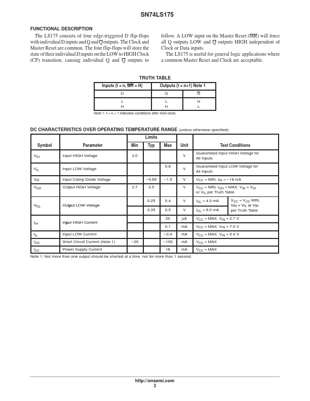
The Clock and Master Reset are common. The four flip-flops will store the state of their individual D inputs on the LOW to HIGH Clock (CP) transition, causing individual Q and Q outputs to follow. A LOW input on the Master Reset (MR) will force all Q outputs LOW and Q outputs HIGH independent of Clock or Data inputs. The LS175 is useful for general logic applications where a common Master Reset and Clock are acceptable. TRUTH TABLE Inputs (t = n, MR = H) D L H Outputs (t = n+1) Note 1 Q L H Q H L Note 1: t = n + 1 indicates conditions after next clock. DC CHARACTERISTICS OVER OPERATING TEMPERATURE RANGE (unless otherwise specified) Limits Symbol VIH VIL VIK VOH Parameter Input HIGH Voltage Input LOW Voltage Input Clamp Diode Voltage Output HIGH Voltage 2.7 – 0.65 3.5 0.25 VOL O Output LOW Voltage 0.35 IIH IIL IOS ICC Input HIGH Current 0.1 Input LOW Current Short Circuit Current (Note 1) Power Supply Current – 20 – 0.4 – 100 18 0.5 20 V µA mA mA mA mA IOL = 8.0 mA 0.4 Min 2... onsemi