onsemi DAN222
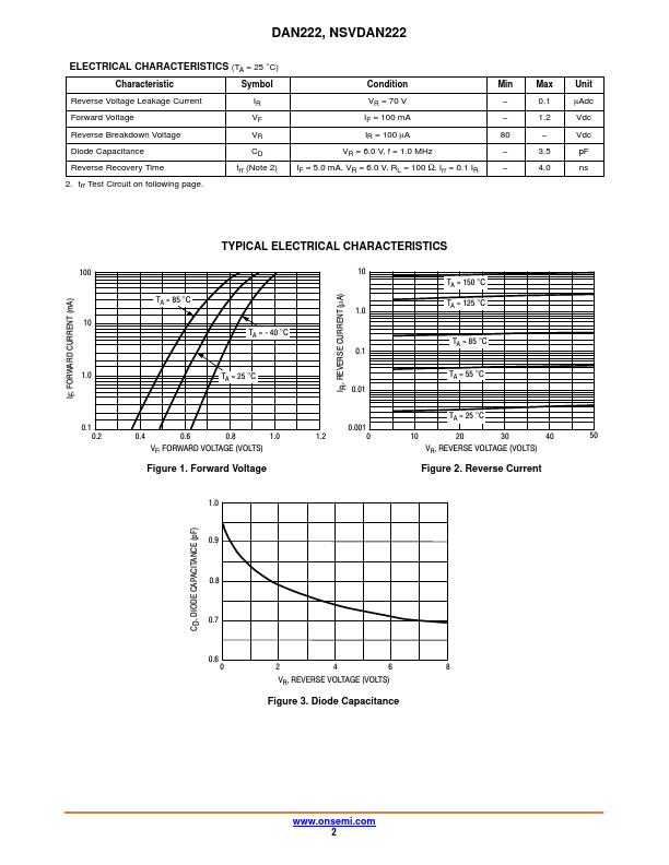
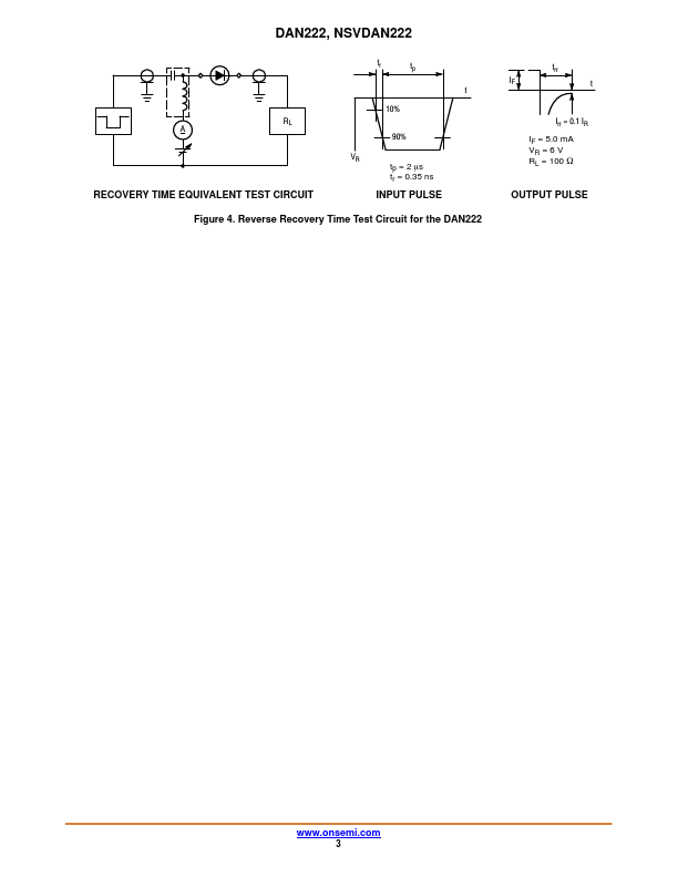
the DAN222 trr IF t Irr = 0.1 IR IF = 5.0 mA VR = 6 V RL = 100 W OUTPUT PULSE 3 MECHANICAL CASE OUTLINE PACKAGE DIMENSIONS SC75−3 1.60x0.80x0.80, 1.00P CASE 463 ISSUE H DATE 01 FEB 2024 GENERIC MARKING DIAGRAM* XXM G 1 XX = Specific Device Code M = Date Code G = Pb−Free Package *This information is generic.| Part No. | DAN222 |
|---|---|
| Datasheet | DAN222 Download |
| Manufacturer |  onsemi |
| Description | Common Cathode Silicon Dual Switching Diode |
| Buy | Stock & Price |
FEATURES
● Fast trr● Low CD
● NSV Prefix for Automotive and Other
APPLICATIONS
Requiring Unique Site and Control Change Requirements; AEC-Q101 Qualified and PPAP Capable● These Devices are Pb-Free, Halogen Free/BFR Free and are RoHS Compliant
MAXIMUM RATINGS
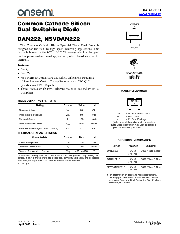
(TA = 25 °C) Rating Symbol Value Unit Reverse Voltage VR Peak Reverse Voltage VRM Forward Current IF Peak Forward Current IFM Peak Forward Surge Current (Note 1) IFSM THERMAL CHARACTERISTICS 80 Vdc 80 Vdc 100 mAdc 300 mAdc 2.0 Adc Characteristic Symbol Max Unit Power Dissipation PD 150 mW Junction Temperature TJ 150 °C/W Storage Temperature Range Tstg −55 to +150 °C Stresses exceeding those listed in theMAXIMUM RATINGS
table may damage the device. If any of these limits are exceeded, device functionality should not be assumed, damage may occur and reliability may be affected. 1. t = 1 ms DATA SHEET CATHODE 3 1 2 ANODE 1 SC-75/SOT-416 CASE 463 STYLE 3 MARKING DIAGRAM N9 M G G 1 N9 = Specific Device Code M = Date Code* G = Pb-Free Package (Note: Microdot may be in either location) *Date Code orientation may vary depending upon manufacturing location.