onsemi FDC2612
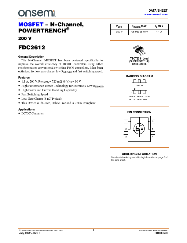
This N−Channel MOSFET has been designed specifically to improve the overall efficiency of DC/DC converters using either synchronous or conventional switching PWM controllers. It has been optimized for low gate charge, low RDS(ON) and fast switching speed.| Part No. | FDC2612 |
|---|---|
| Datasheet | FDC2612 Download |
| Manufacturer |  onsemi |
| Description | N-Channel MOSFET |
| Buy | Stock & Price |
GENERAL DESCRIPTION
FEATURES
● 1.1 A, 200 V. RDS(ON) = 725 mW @ VGS = 10 V● High Performance Trench Technology for Extremely Low RDS(ON)
● High Power and Current Handling Capability
● Fast Switching Speed
● Low Gate Charge (8 nC Typical)
● This Device is Pb−Free, Halide Free and is RoHS Compliant
APPLICATIONS
● DC/DC Converter DATA SHEET VDSS 200 V RDS(ON) MAX 725 mW @ 10 V ID MAX 1.1 A DDS D DG TSOT23 6−Lead (SUPERSOTt−6) CASE 419BL MARKING DIAGRAM 262 M 1 262 = Device Code M = Date Code PIN CONNECTION 1 6 2 5 3 4 ORDERING INFORMATION See detailed ordering and shipping information on page 6 of this data sheet. © Semiconductor Components Industries, LLC, 2002 1 July, 2022 − Rev. 3 Publication Order Number: FDC2612/D FDC2612ABSOLUTE MAXIMUM RATINGS
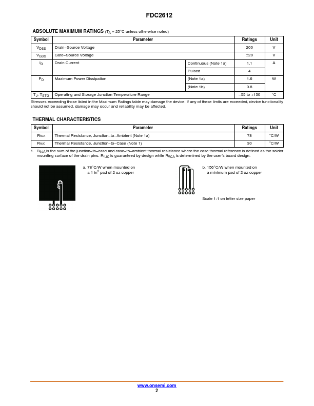
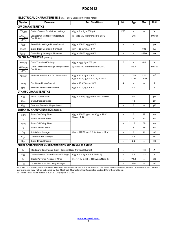
(TA = 25°C unless otherwise noted) Symbol Parameter Ratings Unit VDSS VGSS ID Drain−Source Voltage Gate−Source Voltage Drain Current 200 V ±20 V Continuous (Note 1a) 1.1 A Pulsed 4 PD Maximum Power Dissipation (Note 1a) (Note 1b) 1.6 W 0.8...