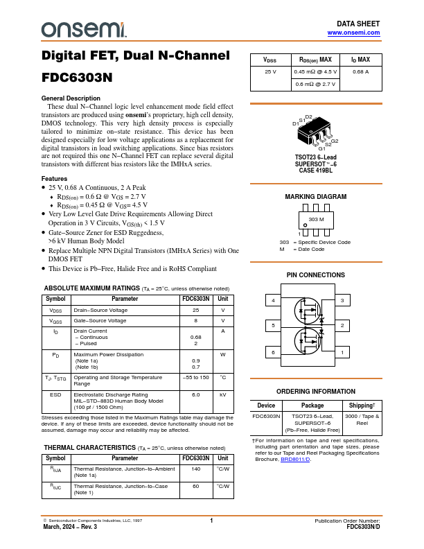
Datasheet4U Logo Datasheet4U.com

FDC6303N - Dual N-Channel Digital FET

General Description

These dual N

transistors are produced using onsemi’s proprietary, high cell density, DMOS technology.

state resistance.

Key Features

  • 25 V, 0.68 A Continuous, 2 A Peak.
  • RDS(on) = 0.6 W @ VGS = 2.7 V.
  • RDS(on) = 0.45 W @ VGS= 4.5 V.
  • Very Low Level Gate Drive Requirements Allowing Direct Operation in 3 V Circuits, VGS(th) < 1.5 V.
  • Gate.
  • Source Zener for ESD Ruggedness, >6 kV Human Body Model.
  • Replace Multiple NPN Digital Transistors (IMHxA Series) with One DMOS FET.
  • This Device is Pb.
  • Free, Halide Free and is RoHS Compliant.

📥 Download Datasheet

Datasheet Details

Part number FDC6303N
Manufacturer onsemi
File Size 263.56 KB
Description Dual N-Channel Digital FET
Datasheet download datasheet FDC6303N Datasheet

Full PDF Text Transcription (Reference)

The following content is an automatically extracted verbatim text from the original manufacturer datasheet and is provided for reference purposes only.

View original datasheet text
DATA SHEET www.onsemi.com Digital FET, Dual N-Channel FDC6303N General Description These dual N−Channel logic level enhancement mode field effect transistors are produced using onsemi’s proprietary, high cell density, DMOS technology. This very high density process is especially tailored to minimize on−state resistance. This device has been designed especially for low voltage applications as a replacement for digital transistors in load switching applications. Since bias resistors are not required this one N−Channel FET can replace several digital transistors with different bias resistors like the IMHxA series. Features • 25 V, 0.68 A Continuous, 2 A Peak ♦ RDS(on) = 0.6 W @ VGS = 2.7 V ♦ RDS(on) = 0.45 W @ VGS= 4.