onsemi FDC6310P
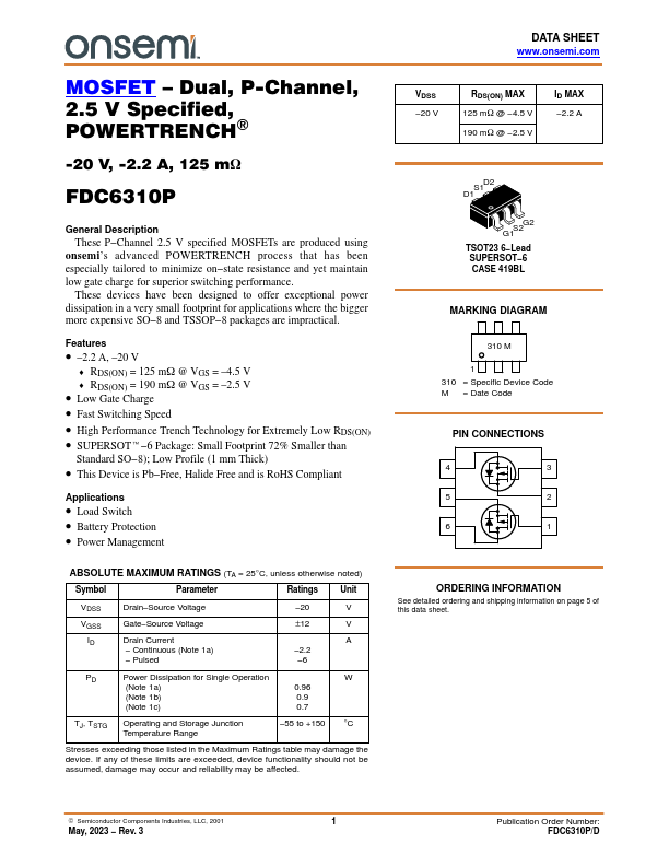
This Device is Pb−Free, Halide Free and is RoHS Compliant Applications • Load Switch • Battery Protection • Power Management ABSOLUTE MAXIMUM RATINGS (TA = 25°C, unless otherwise noted) Symbol Parameter Ratings Unit VDSS VGSS ID Drain−Source Voltage Gate−Source Voltage Drain Current − Continuous (Note 1a) − Pulsed −20 V ±12 V A −2.2 −6 PD Power Dissipation for Single Operation W (Note 1a) 0.96 (Note 1b) 0.9 (Note 1c) 0.7 TJ, TSTG Operating and Storage Junction Temperature Range −55 to +150 °C Stresses exceeding those listed in the Maximum Ratings table may damage the device.| Part No. | FDC6310P |
|---|---|
| Datasheet | FDC6310P Download |
| Manufacturer |  onsemi |
| Description | Dual P-Channel MOSFET |
| Buy | Stock & Price |
GENERAL DESCRIPTION
These P−Channel 2.5 V specified MOSFETs are produced using onsemi’s advanced POWERTRENCH process that has been especially tailored to minimize on−state resistance and yet maintain low gate charge for superior switching performance. These devices have been designed to offer exceptional power dissipation in a very small footprint for applications where the bigger more expensive SO−8 and TSSOP−8 packages are impractical.FEATURES
● –2.2 A, –20 V ♦ RDS(ON) = 125 mW @ VGS = –4.5 V ♦ RDS(ON) = 190 mW @ VGS = –2.5 V● Low Gate Charge
● Fast Switching Speed
● High Performance Trench Technology for Extremely Low RDS(ON)
● SUPERSOTt−6 Package: Small Footprint 72% Smaller than Standard SO−8); Low Profile (1 mm Thick)
● If any of these limits are exceeded, device functionality should not be assumed, damage may occur and reliability may be affected. DATA SHEET VDSS −20 V RDS(ON) MAX 125 mW @ −4.5 V 190 mW @ −2.5 V ID MAX −2.2 A D1S1D2 G1S2G2 TSOT23 6−Lead SUPERSOT−6 CASE 419BL M...

