onsemi FDC6327C
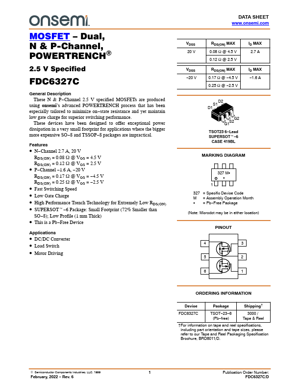
This is a Pb−Free Device Applications • DC/DC Converter • Load Switch • Motor Driving DATA SHEET VDSS 20 V VDSS −20 V RDS(ON) MAX 0.08 W @ 4.5 V 0.12 W @ 2.5 V RDS(ON) MAX 0.17 W @ −4.5 V 0.25 W @ −2.5 V ID MAX 2.7 A ID MAX −1.6 A D2 S1 D1 G2 G1S2 TSOT23 6−Lead SUPERSOTt−6 CASE 419BL MARKING DIAGRAM 327 MG G 1 327 = Specific Device Code M = Assembly Operation Month G = Pb−Free Package (Note: Microdot may be in either location) PINOUT 4 3 5 2 6 1 ORDERING INFORMATION Device Package Shipping† FDC6327C TSOT−23−6 (Pb−free) 3000 / Tape & Reel †For information on tape and reel specifications...| Part No. | FDC6327C |
|---|---|
| Datasheet | FDC6327C Download |
| Manufacturer |  onsemi |
| Description | Dual-Channel MOSFET |
| Buy | Stock & Price |
GENERAL DESCRIPTION
These N & P−Channel 2.5 V specified MOSFETs are produced using onsemi’s advanced POWERTRENCH process that has been especially tailored to minimize on−state resistance and yet maintain low gate charge for superior switching performance. These devices have been designed to offer exceptional power dissipation in a very small footprint for applications where the bigger more expensive SO−8 and TSSOP−8 packages are impractical.FEATURES
● N−Channel 2.7 A, 20 V RDS(ON) = 0.08 W @ VGS = 4.5 V RDS(ON) = 0.12 W @ VGS = 2.5 V● P−Channel −1.6 A, −20 V RDS(ON) = 0.17 W @ VGS = −4.5 V RDS(ON) = 0.25 W @ VGS = −2.5 V
● Fast Switching Speed
● Low Gate Charge
● High Performance Trench Technology for Extremely Low RDS(ON)
● SUPERSOTt−6 Package: Small Footprint (72% Smaller than SO−8); Low Profile (1 mm Thick)
● This is a Pb−Free Device
APPLICATIONS
● DC/DC Converter● Load Switch
● Motor Driving DATA SHEET VDSS 20 V VDSS −20 V RDS(ON) MAX 0.08 W @ 4.5 V 0.12 W @ 2.5 V RDS(ON) MAX 0.

