onsemi FDC653N
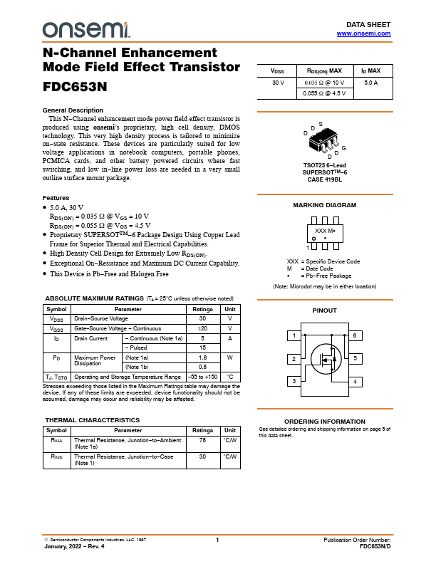
This N−Channel enhancement mode power field effect transistor is produced using onsemi’s proprietary, high cell density, DMOS technology. This very high density process is tailored to minimize on−state resistance.| Part No. | FDC653N |
|---|---|
| Datasheet | FDC653N Download |
| Manufacturer |  onsemi |
| Description | N-Channel MOSFET |
| Buy | Stock & Price |
GENERAL DESCRIPTION
These devices are particularly suited for low voltage applications in notebook computers, portable phones, PCMICA cards, and other battery powered circuits where fast switching, and low in−line power loss are needed in a very small outline surface mount package.FEATURES
● 5.0 A, 30 V RDS(ON) = 0.035 W @ VGS = 10 V RDS(ON) = 0.055 W @ VGS = 4.5 V● Proprietary SUPERSOTTM−6 Package Design Using Copper Lead Frame for Superior Thermal and Electrical Capabilities.
● High Density Cell Design for Extremely Low RDS(ON).
● Exceptional On−Resistance and Maximum DC Current Capability.
● This Device is Pb−Free and Halogen Free
ABSOLUTE MAXIMUM RATINGS
(TA = 25°C unless otherwise noted) Symbol Parameter Ratings Unit VDSS Drain−Source Voltage 30 V VGSS Gate−Source Voltage − Continuous ±20 V ID Drain Current − Continuous (Note 1a) 5 A − Pulsed 15 PD Maximum Power (Note 1a) Dissipation (Note 1b) 1.6 W 0.8 TJ, TSTG Operating and Storage Temperature Range −55 to +150 °C Stresses exceeding those listed in theMAXIMUM RATINGS
table may damage the device.
