onsemi FDC6561AN
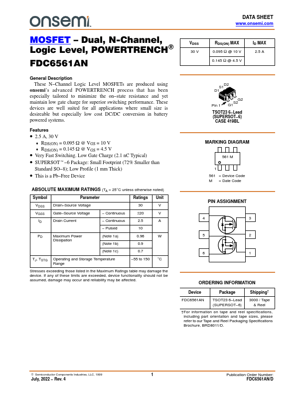
This is a Pb−Free Device ABSOLUTE MAXIMUM RATINGS (TA = 25°C unless otherwise noted) Symbol Parameter Ratings Unit VDSS Drain−Source Voltage 30 V VGSS Gate−Source Voltage − Continuous ±20 V ID Drain Current − Continuous 2.5 A − Pulsed 10 PD Maximum Power Dissipation (Note 1a) (Note 1b) 0.96 W 0.9 (Note 1c) 0.7 TJ, TSTG Operating and Storage Temperature Range −55 to 150 °C Stresses exceeding those listed in the Maximum Ratings table may damage the device.FDC6561AN Specifications
- Package : SOT-23-6
- Mount Type : Surface Mount
- Current Rating : 2.5A
- Breakdown Voltage : 30V
- RDS(on) Max : 95mΩ
- Input Capacitance : 220pF
- Terminals : 6
- Rise Time : 10ns
- Max Power Dissipation : 960mW
- Max Operating Temp : 150°C
- Min Operating Temp : -55°C
Source:
Octopart
| Part No. | FDC6561AN |
|---|---|
| Datasheet | FDC6561AN Download |
| Manufacturer |  onsemi |
| Description | Dual N-Channel MOSFET |
| Buy | Stock & Price |
GENERAL DESCRIPTION
These N−Channel Logic Level MOSFETs are produced using onsemi’s advanced POWERTRENCH process that has been especially tailored to minimize the on−state resistance and yet maintain low gate charge for superior switching performance. These devices are well suited for all applications where small size is desireable but especially low cost DC/DC conversion in battery powered systems.FEATURES
● 2.5 A, 30 V ♦ RDS(ON) = 0.095 W @ VGS = 10 V ♦ RDS(ON) = 0.145 W @ VGS = 4.5 V● Very Fast Switching. Low Gate Charge (2.1 nC Typical)
● SUPERSOTt−6 Package: Small Footprint (72% Smaller than Standard SO−8); Low Profile (1 mm Thick)
● If any of these limits are exceeded, device functionality should not be assumed, damage may occur and reliability may be affected. D2 S1 D1 G2 Pin 1 G1S2 TSOT23 6−Lead (SUPERSOT−6) CASE 419BL MARKING DIAGRAM 561 M 1 561 = Device Code M = Date Code PIN ASSIGNMENT 4 3 5 2 6 1 ORDERING INFORMATION Device Package Shipping† FDC6561AN TSOT23 6−Lead 3000 /...

