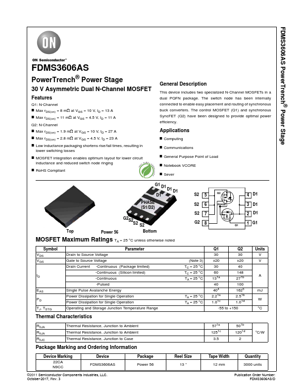
FEATURES
Q1: N-Channel Max rDS(on) = 8 mΩ at VGS = 10 V, ID = 13 A Max rDS(on) = 11 mΩ at VGS = 4.5 V, ID = 11 A Q2: N-Channel Max rDS(on) = 1.9 mΩ at VGS = 10 V, ID = 27 A Max rDS(on) = 2.8 mΩ at VGS = 4.5 V, ID = 23 A Low inductance packaging shortens rise/fall times, resulting in lower switching losses MOSFET integration enables optimum layout for lower circuit inductance and reduced switch node ringing RoHS Compliant GENERAL DESCRIPTION
The control MOSFET (Q1) and synchronous SyncFET (Q2) have been designed to provide optimal power efficiency. APPLICATIONS
Computing Communications General Purpose Point of Load Notebook VCORE Sever G1 D1 D1 D1 D1 PHASE (S1/D2) G2S2S2 S2 Top Power 56 Bottom MOSFET MAXIMUM RATINGS
TA = 25 °C unless otherwise noted Symbol VDS VGS ID EAS PD TJ, TSTG Parameter Drain to Source Voltage Gate to Source Voltage Drain Current -Continuous (Package limited) -Continuous (Silicon limited) -Continuous -Pulsed Single Pulse Avalanche Energy Po... onsemi