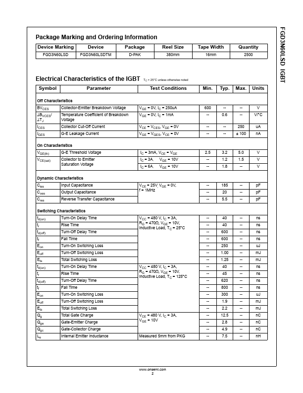
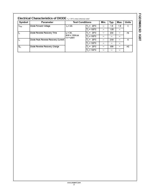
onsemi FGD3N60LSD
The device is designed for applica-tions where very low On-Voltage Drop is a required feature. for Soldering Purposes, 1/8” from Case for 5 Seconds Notes : (1) Repetitive rating : Pulse width limited by max.| Part No. | FGD3N60LSD |
|---|---|
| Datasheet | FGD3N60LSD Download |
| Manufacturer |  onsemi |
| Description | IGBT |
| Buy | Stock & Price |
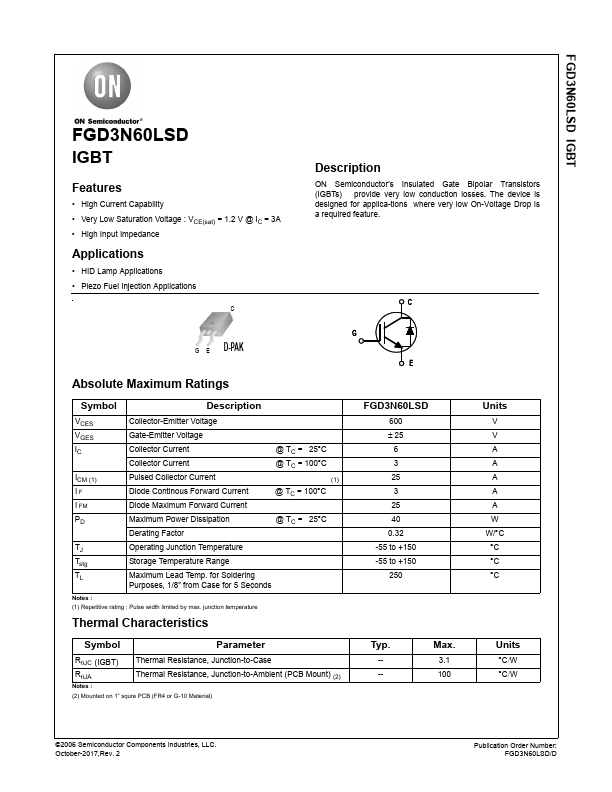
FEATURES
● High Current Capability● Very Low Saturation Voltage : VCE(sat) = 1.2 V @ IC = 3A
● High Input Impedance
APPLICATIONS
● HID LampAPPLICATIONS
● Piezo Fuel InjectionAPPLICATIONS
CDESCRIPTION
ON Semiconductor's Insulated Gate Bipolar Transistors (IGBTs) provide very low conduction losses. C G E D-PAK G EABSOLUTE MAXIMUM RATINGS
SymbolDESCRIPTION
VCES VGES IC ICM (1) IF I FM Collector-Emitter Voltage Gate-Emitter Voltage Collector Current Collector Current Pulsed Collector Current Diode Continous Forward Current Diode Maximum Forward Current @ TC = 25°C @ TC = 100°C (1) @ TC = 100°C PD Maximum Power Dissipation Derating Factor @ TC = 25°C TJ Operating Junction Temperature Tstg Storage Temperature Range TL Maximum Lead Temp. junction temperature Thermal Characteristics FGD3N60LSD 600 ± 25 6 3 25 3 25 40 0.32 -55 to +150 -55 to +150 250 Symbol Parameter RθJC (IGBT) Thermal Resistance, Junction-to-Case RθJA Thermal Resistance, Junction-to-Ambient (PCB Mount) (2) Notes : (2) Mounted on 1” squre PCB (FR4 or G-10 Material) Typ. --- Max.