onsemi KSC5027
NPN Silicon Transistor
| Part No. | KSC5027 |
|---|---|
| Datasheet | KSC5027 Download |
| Manufacturer |  onsemi |
| Description | NPN Silicon Transistor |
| Buy | Stock & Price |
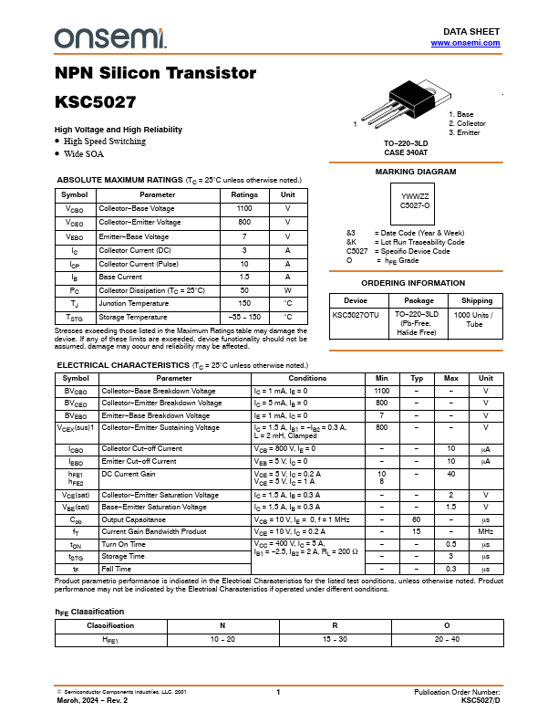
ABSOLUTE MAXIMUM RATINGS
(TC = 25°C unless otherwise noted.) Symbol Parameter Ratings Unit VCBO Collector−Base Voltage 1100 V VCEO Collector−Emitter Voltage 800 V VEBO Emitter−Base Voltage 7 V IC Collector Current (DC) 3 A ICP Collector Current (Pulse) 10 A IB Base Current 1.5 A PC Collector Dissipation (TC = 25°C) 50 W TJ Junction Temperature 150 °C TSTG Storage Temperature −55 ~ 150 °C Stresses exceeding those listed in theMAXIMUM RATINGS
table may damage the device. If any of these limits are exceeded, device functionality should not be assumed, damage may occur and reliability may be affected. T 1. Base 1 2. Collector 3. Emitter TO−220−3LD CASE 340AT MARKING DIAGRAM YWWZZ C5027-O &3 &K C5027 O = Date Code (Year & Week) = Lot Run Traceability Code = Specific Device Code = hFE Grade ORDERING INFORMATION Device KSC5027OTU Package TO−220−3LD (Pb-Free, Halide Free) Shipping 1000 Units / TubeELECTRICAL CHARACTERISTICS
(TC = 25°C unless otherwise noted.) Symbol Parameter Conditions Min...