NCP51752
NCP51752 is 4.5-A/9-A Isolated Single Channel Gate Driver manufactured by onsemi.
3.75 k VRMS, 4.5-A/9-A Isolated Single Channel Gate Driver with Integrated Negative Bias Control
The NCP51752 is a family of isolated single- channel gate driver with 4.5- A/9- A source and sink peak current respectively. They are designed for fast switching to drive power MOSFETs and Si C MOSFET power switches. The NCP51752 offers short and matched propagation delays. For improved reliability, d V/dt immunity and even faster turn- off, the NCP51752 has an innovative embedded negative bias rail mechanism. The NCP51752 offers other important protection function such as independent under- voltage lockout for both- side driver. Its Vcc UVLO threshold is referenced to GND2 for true UVLO regardless of VEE level. The NCP51752 is available in a 4 mm SOIC- 8 package and can support isolation voltage up to 3.75 k VRMS.
Features
- Feature Options
- VCC UVLO Referenced to GND2
- Built- in Negative Bias between GND2 and VEE Pins
Selectable Negative Bias Levels via Trim
- 3- V to 20- V Input Supply Voltage
- Output Supply Voltage from 6.5 V to 30 V with 6- V and 8- V for
MOSFET, 12- V and 17- V for Si C, Threshold
- 4.5- A Peak Source, 9- A Peak Sink Output Current Capability
- Minimum CMTI of 200 V/ns d V/dt
- Negative 5- V Handling Capability on Input Pins
- Propagation Delay Typical 36 ns with
- 5 ns Max Delay Matching
- Isolation & Safety
- 3.75 k VRMS Isolation for 1 Minute (per UL1577 Requirements) (Planned)
- CQC Certification per GB4943.1- 2011 (Planned)
- SGS FIMO Certification per IEC 62386- 1 (Planned)
Typical Applications
- Motor Drives
- Isolated Converters in DC- DC and AC- DC Power Supply
- Server, Tele, and Industrial Infrastructure
DATA SHEET .onsemi.
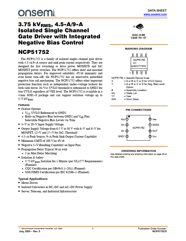
SOIC- 8 NB CASE 751- 07
MARKING DIAGRAM
NCP51752 XY D AWLYYWW
NCP51752 = Specific Device Code
= A or B or C or D for UVLO Option
= A or B or C or D for Neg. Bias...