onsemi NCP6361
The NCP6361, a PWM synchronous step−down DC−to−DC converter, is optimized for supplying RF Power Amplifiers (PAs) used in 3G/4G wireless systems (Mobile / Smart Phones, Tablets,…) powered by single−cell Lithium−Ion batteries. The device is able to deliver up to 2 A current in bypass mode and 800 mA in buck mode. The output voltage is monitorable from 0.4 V to 3.5 V by an analog control pin VCON.| Part No. | NCP6361 |
|---|---|
| Datasheet | NCP6361 Download |
| Manufacturer |  onsemi |
| Description | Buck Converter |
| Buy | Stock & Price |
FEATURES
● Input Voltage from 2.5 V to 5.5 V for Battery PoweredAPPLICATIONS
● Adjustable Output Voltage (0.4 V to 3.50 V)● 3.429 / 6 MHz Selectable Switching Frequency
● Uses 470 nH Inductor and 4.7 mF Capacitor for Optimized Footprint and Solution Thickness
● PFM /PWM/Bypass Automatic Mode Change for High Efficiency
● Low 45 mA Quiescent Current
● Thermal Protections to Avoid Damage of the IC
● Small 1.36 x 1.22 mm / 0.4 mm Pitch CSP Package
● This is a Pb−Free Device Typical
APPLICATIONS
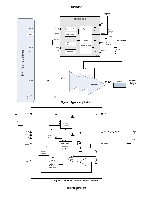
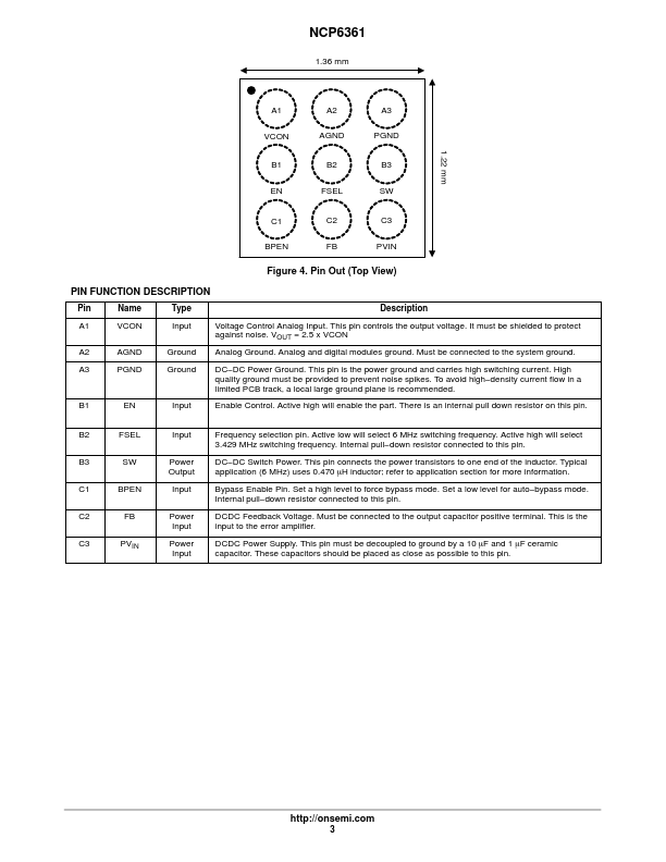
● 3G / 4G Wireless Systems, Smart−Phones and Webtablets NCP6361 VBATT Battery or System Supply Bypass Enable BPEN Bypass Control Bypass FB VCON AGND FSEL EN Vout Control Thermal Protection Enabling DCDC 1.0A 3.43/6.00 MHz PVIN 10uF SW 0.47uH PGND VOUT 4.7uF Figure 1. NCP6361 Block Diagram © Semiconductor Components Industries, LLC, 2014 April, 2014 − Rev. 5 1 Publication Order Number: NCP6361/D GPI /O DAC GPI /O GPI /O BPEN VCON AGND FSEL EN NCP6361 NCP6361 Bypass Control Vout Control Thermal Prot...