onsemi NCV511
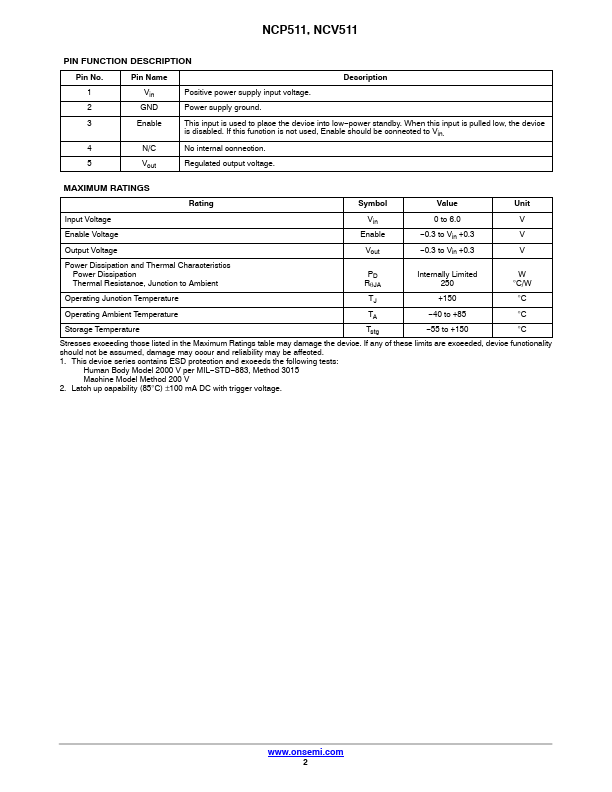
This input is used to place the device into low−power standby. When this input is pulled low, the device ÁÁÁÁÁÁÁÁÁÁÁÁÁÁÁÁÁÁÁÁÁÁÁÁÁÁÁÁÁÁÁÁÁis disabled.| Part No. | NCV511 |
|---|---|
| Datasheet | NCV511 Download |
| Manufacturer |  onsemi |
| Description | Low-Dropout Voltage Regulator |
| Buy | Stock & Price |
FEATURES
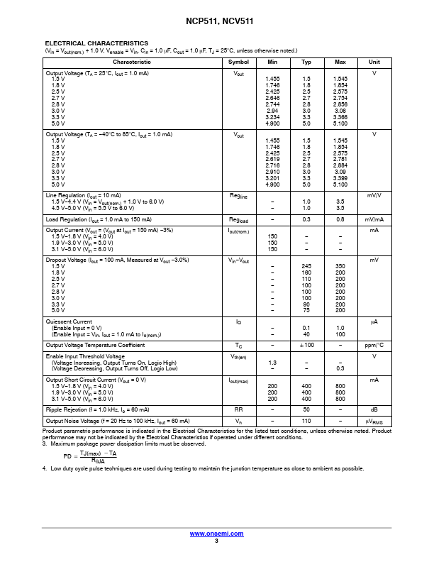
● Low Quiescent Current of 40 mA Typical● Low Dropout Voltage of 100 mV at 100 mA
● Excellent Line and Load Regulation
● Maximum Operating Voltage of 6.0 V
● Low Output Voltage Option
● High Accuracy Output Voltage of 2.0%
● Industrial Temperature Range of −40°C to 85°C
● NCV Prefix for Automotive and Other
APPLICATIONS
Requiring Unique Site and Control Change Requirements; AEC−Q100 Qualified and PPAP Capable● These are Pb−Free Devices Typical
APPLICATIONS
● Cellular Phones● Battery Powered Instruments
● Hand−Held Instruments
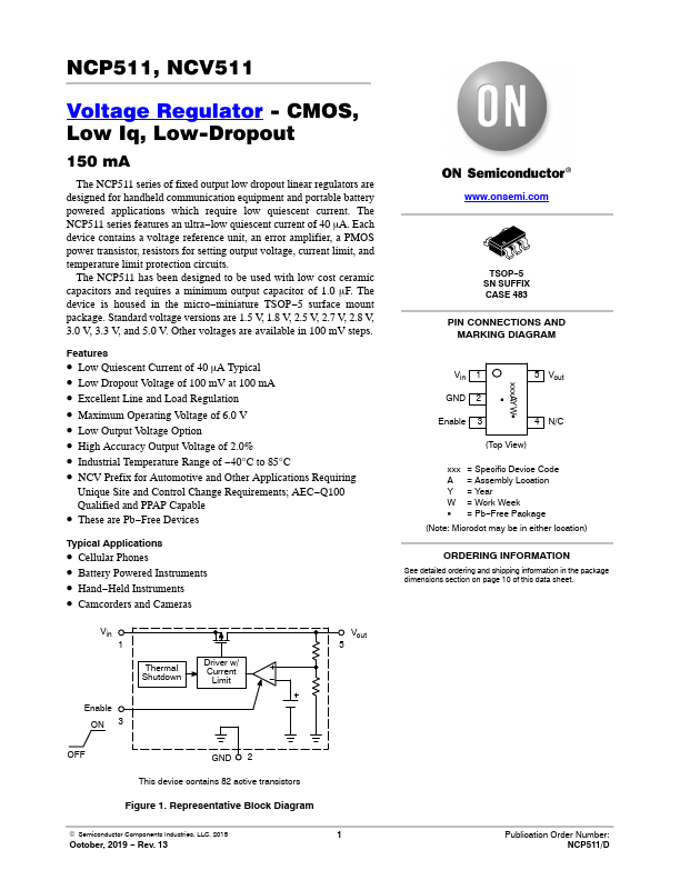
● Camcorders and Cameras Vin 1 Thermal Shutdown Driver w/ Current Limit Vout 5 Enable ON 3 OFF GND 2 This device contains 82 active transistors Figure 1. Representative Block Diagram © Semiconductor Components Industries, LLC, 2015 October, 2019 − Rev. 13 1 TSOP−5 SN SUFFIX CASE 483 PIN CONNECTIONS AND MARKING DIAGRAM xxxAYWG G Vin 1 GND 2 5 Vout Enable 3 4 N/C (Top View) xxx = Specific Device Code A = Assembly Location Y = Year W = Work Week G = Pb−Fr...