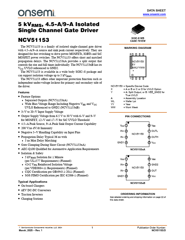
Datasheet4U Logo Datasheet4U.com

NCV51153 - 4.5-A/9-A Isolated Single Channel Gate Driver

General Description

Pin No.

3 3 GND1 4 4 VCC 5 5 OUTH 6 6 OUTL 7 GND2

Description Input-side Supply Voltage.

Key Features

  • Feature Options.
  • Separated Outputs (NCV51153xA).
  • Wide Bias Voltage Range Including Negative VEE and VCC UVLO Referenced to GND2 (NCV51153xB).
  • 3.
  • V to 20.
  • V Input Supply Voltage.
  • Output Supply Voltage from 6.5 V to 30 V with 6.
  • V and 9.
  • V for MOSFET, 12.
  • V and 17.
  • V for SiC UVLO Threshold.
  • 4.5.
  • A Peak Source, 9.
  • A Peak Sink Output Current Capability.
  • 200 V/ns dV/dt Immunity.

📥 Download Datasheet

Datasheet Details

Part number NCV51153
Manufacturer onsemi
File Size 2.20 MB
Description 4.5-A/9-A Isolated Single Channel Gate Driver
Datasheet download datasheet NCV51153 Datasheet

Full PDF Text Transcription (Reference)

The following content is an automatically extracted verbatim text from the original manufacturer datasheet and is provided for reference purposes only.

View original datasheet text
5 kVRMS, 4.5-A/9-A Isolated Single Channel Gate Driver NCV51153 The NCV51153 is a family of isolated single-channel gate driver with 4.5−A/9−A source and sink peak current respectively. They are designed for fast switching to drive power MOSFETs, IGBTs and SiC MOSFET power switches. The NCV51153 offers short and matched propagation delays. The NCV51153xA provides a split output that controls the rise and fall times individually. The NCV51153xB has its VCC UVLO referenced to GND2. The NCV51153 is available in a wide body SOIC−8 package and can support isolation voltage up to 5 kVRMS. The NCV51153 offers other important protection function such as independent under-voltage lockout for primary and secondary side of the driver.