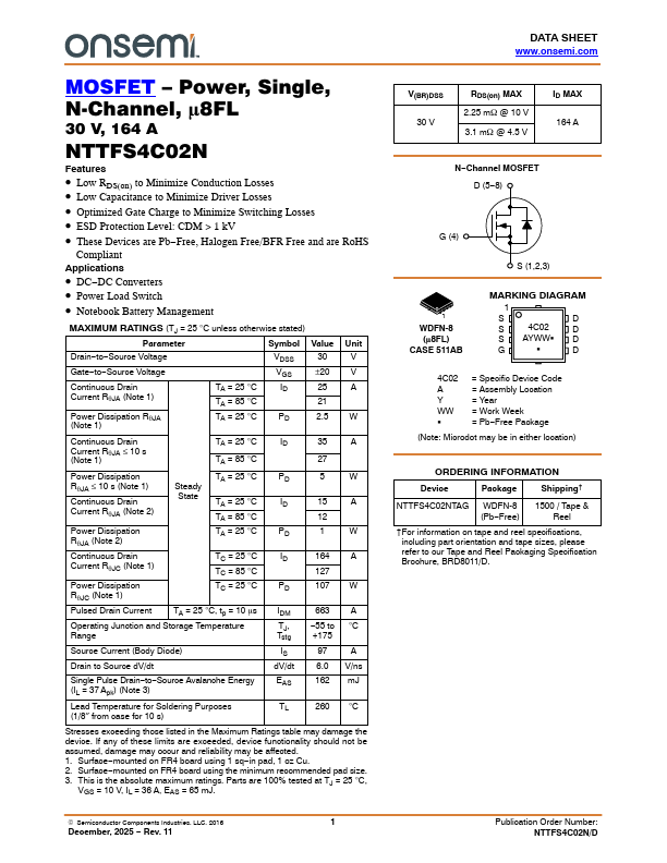
NTTFS4C02N
Features
- Low RDS(on) to Minimize Conduction Losses
- Low Capacitance to Minimize Driver Losses
- Optimized Gate Charge to Minimize Switching Losses
- ESD Protection Level: CDM > 1 k V
- These Devices are Pb- Free, Halogen Free/BFR Free and are Ro HS pliant
Applications
- DC- DC Converters
- Power Load Switch
- Notebook Battery Management
MAXIMUM RATINGS (TJ = 25 °C unless otherwise stated)
Parameter
Symbol Value Unit
Drain- to- Source Voltage
VDSS
Gate- to- Source Voltage
±20 V
Continuous Drain Current Rq JA (Note 1)
TA = 25 °C
TA = 85 °C
Power Dissipation Rq JA (Note 1)
TA = 25 °C
2.5 W
Continuous Drain Current Rq JA ≤ 10 s (Note 1)
TA = 25 °C
TA = 85 °C
Power Dissipation Rq JA ≤ 10 s (Note 1)
Continuous Drain Current Rq JA (Note 2)
Steady State
TA = 25 °C
TA = 25 °C TA = 85 °C
Power Dissipation Rq JA (Note 2)
TA = 25...