onsemi SN74LS109A
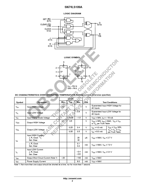
The SN74LS109A consists of two high speed completely independent transition clocked JK flip-flops. The clocking operation is independent of rise and fall times of the clock waveform. The JK design allows operation as a D flip-flop by simply connecting the J and K pins together.| Part No. | SN74LS109A |
|---|---|
| Datasheet | SN74LS109A Download |
| Manufacturer |  onsemi |
| Description | Dual JK Positive Edge-Triggered Flip-Flop |
| Buy | Stock & Price |
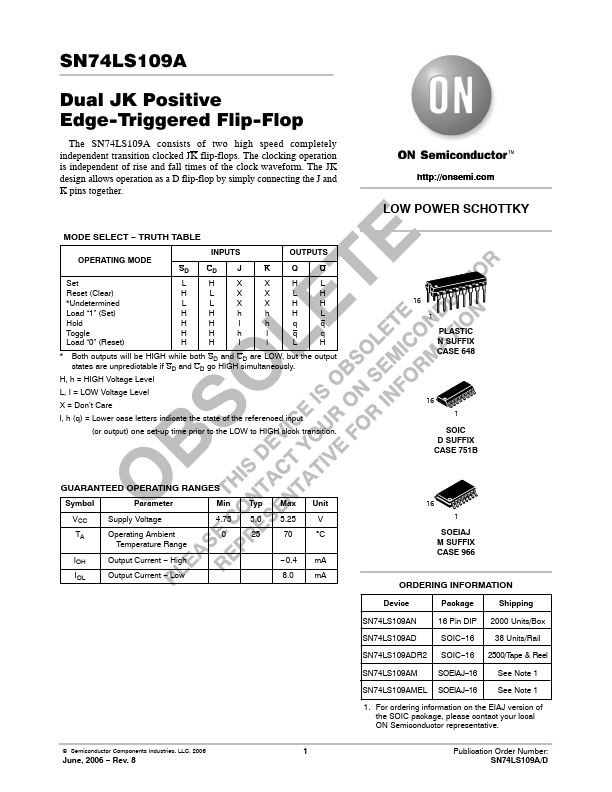
SN74LS109A Dual JK Positive Edge−Triggered Flip−Flop MODE SELECT − TRUTH TABLE OPERATING MODE INPUTS SD CD J OUTPUTS K Q Q Set Reset (Clear) *Undetermined Load “1” (Set) Hold Toggle Load “0” (Reset) L H X X H L H L X X L H L L X X H H H H h h H L H H l h q q H H h l q q H H l l L H * Both outputs will be HIGH while both SD and CD are LOW, but the output states are unpredictable if SD and CD go HIGH simultaneously. H, h = HIGH Voltage Level L, I = LOW Voltage Level X = Don’t Care l, h (q) = Lower case letters indicate the state of the referenced input i, h (q) = (or output) one set-up time prior to the LOW to HIGH clock transition. LOW POWER SCHOTTKY 16 1 PLASTIC N SUFFIX CASE 648 16 1 SOIC D SUFFIX CASE 751B GUARANTEED OPERATING RANGES Symbol Parameter Min Typ Max Unit VCC Supply Voltage TA Operating Ambient Temperature Range 4.75 5.0 5.25 V 0 25 70 °C IOH Output Current − High IOL Output Current − Low −0.4 mA 8.0 mA © Semiconductor Components Industries, LLC, 2006 1 June, 2006 − Rev.