9DB1933 Datasheet
9DB1933 Datasheet (IDT)
IDT
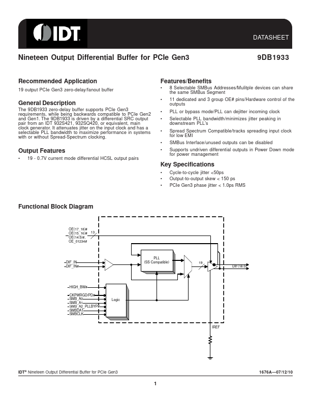
The 9DB1933 zero-delay buffer supports PCIe Gen3 requirements, while being backwards compatible to PCIe Gen2 and Gen1. The 9DB1933 is driven by a differential SRC output pair from an IDT 932S421, 932S.
* 19 - 0.7V current mode differential HCSL output pairs
Features/Benefits
* 8 Selectable SMBus Addresses/Mulitple devices can share the same SMBus Segment
* 11 dedicated and 3 group OE# pins/Hardware control of the outputs
* PLL or bypass mode/PLL can dejitter incoming clock
* Selectable PLL bandwi.
9DB1933 Datasheet (Renesas)
Renesas
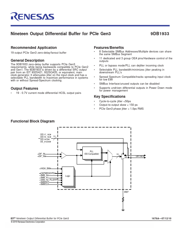
The 9DB1933 zero-delay buffer supports PCIe Gen3 requirements, while being backwards compatible to PCIe Gen2 and Gen1. The 9DB1933 is driven by a differential SRC output pair from an IDT 932S421, 932S.
* 19 - 0.7V current mode differential HCSL output pairs
Features/Benefits
* 8 Selectable SMBus Addresses/Mulitple devices can share the same SMBus Segment
* 11 dedicated and 3 group OE# pins/Hardware control of the outputs
* PLL or bypass mode/PLL can dejitter incoming clock
* Selectable PLL bandwi.