QL2009 Datasheet
QL2009 Datasheet (Unknown Manufacturer)
Unknown Manufacturer

Pin TDI TRSTB TMS TCK TDO STM I/ACLK I/GCLK I I/O VCC GND Function Test Data In for JTAG Active low Reset for JTAG Test Mode Select for JTAG Test Clock for JTAG Test data out for JTAG Special Test Mo.
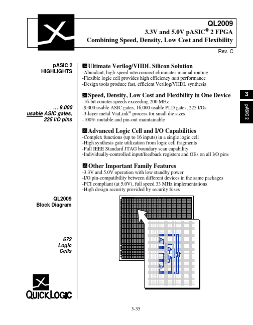
-3.3V and 5.0V operation with low standby power -I/O pin-compatibility between different devices in the same packages -PCI compliant (at 5.0V), full speed 33 MHz implementations -High design security provided by security fuses QL2009 Block Diagram 672 Logic Cells 3-35 QL2009 PRODUCT SUMMARY The Q.
QL2009-XPQ208I Datasheet (Unknown Manufacturer)
Unknown Manufacturer

Pin TDI TRSTB TMS TCK TDO STM I/ACLK I/GCLK I I/O VCC GND Function Test Data In for JTAG Active low Reset for JTAG Test Mode Select for JTAG Test Clock for JTAG Test data out for JTAG Special Test Mo.
-3.3V and 5.0V operation with low standby power -I/O pin-compatibility between different devices in the same packages -PCI compliant (at 5.0V), full speed 33 MHz implementations -High design security provided by security fuses QL2009 Block Diagram 672 Logic Cells 3-35 QL2009 PRODUCT SUMMARY The Q.
QL2009-XPQ208C Datasheet (Unknown Manufacturer)
Unknown Manufacturer
Pin TDI TRSTB TMS TCK TDO STM I/ACLK I/GCLK I I/O VCC GND Function Test Data In for JTAG Active low Reset for JTAG Test Mode Select for JTAG Test Clock for JTAG Test data out for JTAG Special Test Mo.
-3.3V and 5.0V operation with low standby power -I/O pin-compatibility between different devices in the same packages -PCI compliant (at 5.0V), full speed 33 MHz implementations -High design security provided by security fuses QL2009 Block Diagram 672 Logic Cells 3-35 QL2009 PRODUCT SUMMARY The Q.
QL2009-XPF144I Datasheet (Unknown Manufacturer)
Unknown Manufacturer

Pin TDI TRSTB TMS TCK TDO STM I/ACLK I/GCLK I I/O VCC GND Function Test Data In for JTAG Active low Reset for JTAG Test Mode Select for JTAG Test Clock for JTAG Test data out for JTAG Special Test Mo.
-3.3V and 5.0V operation with low standby power -I/O pin-compatibility between different devices in the same packages -PCI compliant (at 5.0V), full speed 33 MHz implementations -High design security provided by security fuses QL2009 Block Diagram 672 Logic Cells 3-35 QL2009 PRODUCT SUMMARY The Q.