93C56
93C56 is 3-Wire Serial EEPROMs manufactured by Atmel.
Features
- Low-voltage and Standard-voltage Operation
- 2.7 (VCC = 2.7V to 5.5V)
- 1.8 (VCC = 1.8V to 5.5V)
- User-selectable Internal Organization
- 1K: 128 x 8 or 64 x 16
- 2K: 256 x 8 or 128 x 16
- 4K: 512 x 8 or 256 x 16
- Three-wire Serial Interface
- 2 MHz Clock Rate (5V)
- Self-timed Write Cycle (10 ms max)
- High Reliability
- Endurance: 1 Million Write Cycles
- Data Retention: 100 Years
- Automotive Grade, Extended Temperature and Lead-Free/Halogen-Free
Devices Available
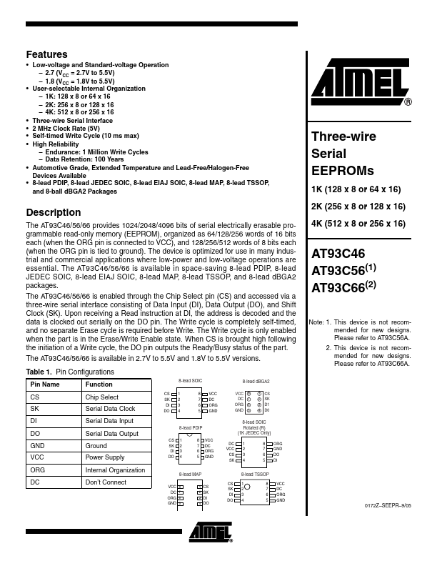
- 8-lead PDIP, 8-lead JEDEC SOIC, 8-lead EIAJ SOIC, 8-lead MAP, 8-lead TSSOP, and 8-ball d BGA2 Packages
Description
The AT93C46/56/66 provides 1024/2048/4096 bits of serial electrically erasable programmable read-only memory (EEPROM), organized as 64/128/256 words of 16 bits each (when the ORG pin is connected to VCC), and 128/256/512 words of 8 bits each (when the ORG pin is tied to ground). The device is optimized for use in many industrial and mercial applications where low-power and low-voltage operations are essential. The AT93C46/56/66 is available in space-saving 8-lead PDIP, 8-lead JEDEC SOIC, 8-lead EIAJ SOIC, 8-lead MAP, 8-lead TSSOP, and 8-lead d BGA2 packages.
The AT93C46/56/66 is enabled through the Chip Select pin (CS) and accessed via a three-wire serial interface consisting of Data Input (DI), Data Output (DO), and Shift Clock (SK). Upon receiving a Read instruction at DI, the address is decoded and the data is clocked out serially on the DO pin. The Write cycle is pletely self-timed, and no separate Erase cycle is required before Write. The Write cycle is only enabled when the part is in the Erase/Write Enable state. When CS is brought high following the initiation of a Write cycle, the DO pin outputs the Ready/Busy status of the part.
The AT93C46/56/66 is available in 2.7V to 5.5V and 1.8V to 5.5V versions.
Table 1. Pin Configurations
Pin Name
Function
CS Chip Select
SK Serial Data Clock
DI Serial Data Input
DO Serial Data Output
Ground
Power...