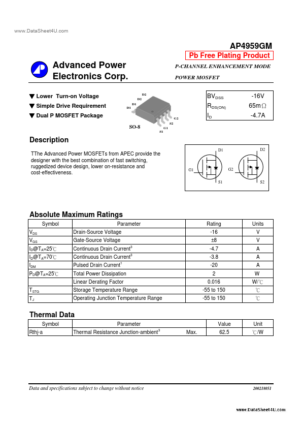
The following content is an automatically extracted verbatim text
from the original manufacturer datasheet and is provided for reference purposes only.
View original datasheet text
www.DataSheet4U.com
AP4959GM
Pb Free Plating Product
Advanced Power Electronics Corp.
▼ Lower Turn-on Voltage ▼ Simple Drive Requirement ▼ Dual P MOSFET Package
SO-8
S1 S2 G1 D1 D1 D2 D2
P-CHANNEL ENHANCEMENT MODE POWER MOSFET
BVDSS RDS(ON)
G2
-16V 65mΩ -4.7A
ID
Description
TThe Advanced Power MOSFETs from APEC provide the designer with the best combination of fast switching, ruggedized device design, lower on-resistance and cost-effectiveness.
D1 D2
G1 S1
G2 S2
Absolute Maximum Ratings
Symbol VDS VGS ID@TA=25℃ ID@TA=70℃ IDM PD@TA=25℃ TSTG TJ Parameter Drain-Source Voltage Gate-Source Voltage Continuous Drain Current Continuous Drain Current Pulsed Drain Current
1 3 3
Rating -16 ±8 -4.7 -3.8 -20 2 0.