Datasheet4U Logo Datasheet4U.com

AS4C256M16D3LB-12BIN - 4Gb DRAM

Datasheet Summary

Description

Clock : CK and CK are differential clock inputs.

All address and control input signals are sampled on the crossing of the positive edge of CK and negative edge of CK.

Features

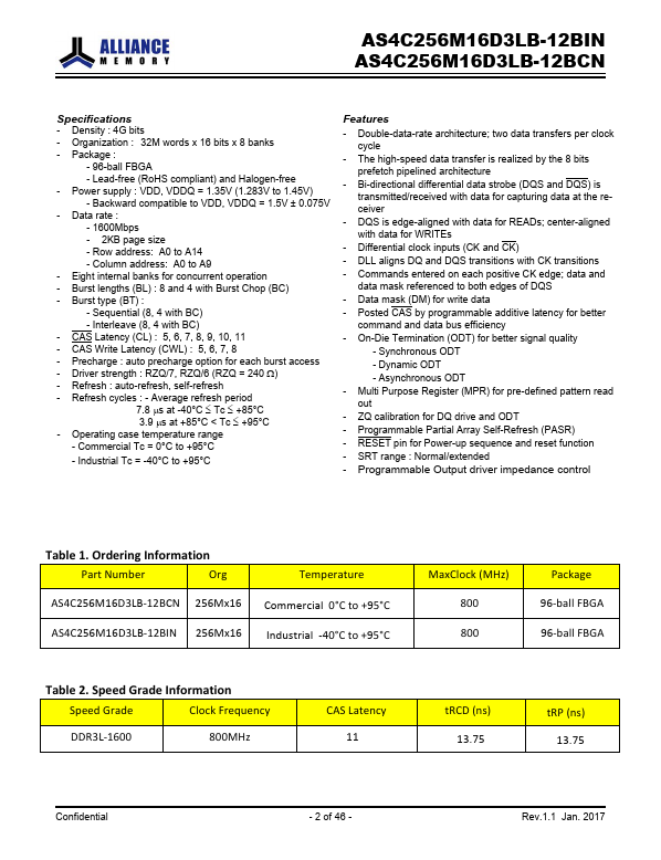
  • - Double-data-rate architecture; two data transfers per clock cycle - The high-speed data transfer is realized by the 8 bits prefetch pipelined architecture - Bi-directional differential data strobe (DQS and DQS) is transmitted/received with data for capturing data at the receiver - DQS is edge-aligned with data for READs; center-aligned with data for WRITEs - Differential clock inputs (CK and CK) - DLL aligns DQ and DQS transitions with CK transitions - Commands entered on each positive CK edge.

📥 Download Datasheet

Datasheet preview – AS4C256M16D3LB-12BIN

Datasheet Details

Part number AS4C256M16D3LB-12BIN
Manufacturer Alliance Semiconductor
File Size 2.37 MB
Description 4Gb DRAM
Datasheet download datasheet AS4C256M16D3LB-12BIN Datasheet
Additional preview pages of the AS4C256M16D3LB-12BIN datasheet.
Other Datasheets by Alliance Semiconductor

Full PDF Text Transcription

Click to expand full text
AS4C256M16D3LB-12BIN AS4C256M16D3LB-12BCN Revision History 4Gb AS4C256M16D3LB - 12BIN/BCN 96 ball FBGA PACKAGE Revision Rev 1.0 Rev 1.1 Details Preliminary datasheet Add Industrial part datasheet Date Apr. 2016 Jan. 2017 Alliance Memory Inc. 511 Taylor Way, San Carlos, CA 94070 TEL: (650) 610-6800 FAX: (650) 620-9211 Alliance Memory Inc. reserves the right to change products or specification without notice Confidential - 1 of 46 - Rev.1.1 Jan. 2017 AS4C256M16D3LB-12BIN AS4C256M16D3LB-12BCN Specifications - Density : 4G bits - Organization : 32M words x 16 bits x 8 banks - Package : - 96-ball FBGA - Lead-free (RoHS compliant) and Halogen-free - Power supply : VDD, VDDQ = 1.35V (1.283V to 1.45V) - Backward compatible to VDD, VDDQ = 1.5V ± 0.
Published: |