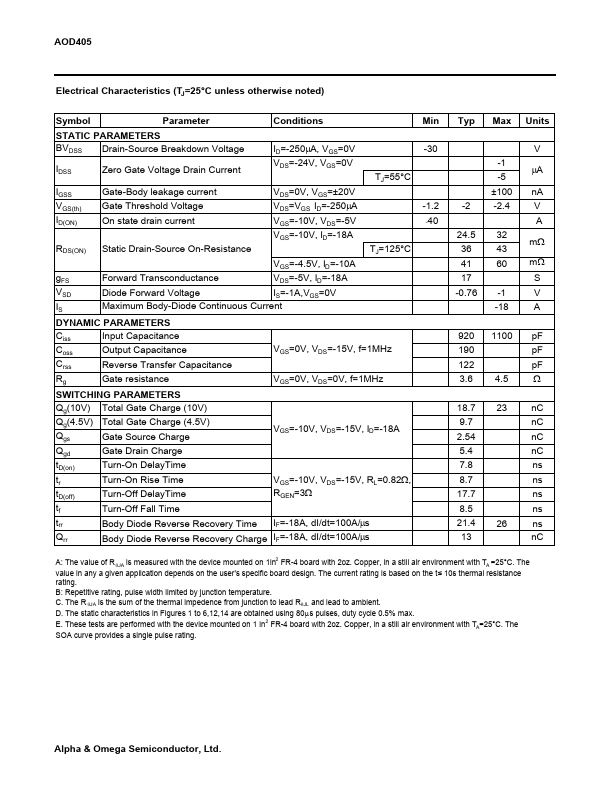
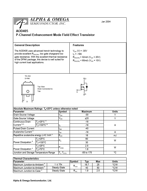
Datasheet4U Logo Datasheet4U.com

AOD405 - P-Channel MOSFET

Description

The AOD405 uses advanced trench technology to provide excellent RDS(ON), low gate chargeand low gate resistance.

With the excellent thermal resistance of the DPAK package, this device is well suited for high current load applications.

Features

  • VDS (V) = -30V ID = -18A RDS(ON) < 32mΩ (VGS = 20V) RDS(ON) < 60mΩ (VGS = 10V) TO-252 D-PAK D Top View Drain Connected to Tab G S GD S Absolute Maximum Ratings TA=25°C unless otherwise noted Parameter Symbol Drain-Source Voltage VDS Gate-Source Voltage VGS Continuous Drain TA=25°C G Current B,G TA=100°C B ID Pulsed Drain Current IDM Avalanche Current C IAR Repetitive avalanche energy L=0.1mH C EAR TC=25°C Power Dissipation B TC=100°C PD TA=25°C Power Dissipation A TA=7.

📥 Download Datasheet

Full PDF Text Transcription (Reference)

The following content is an automatically extracted verbatim text from the original manufacturer datasheet and is provided for reference purposes only.

View original datasheet text
Jan 2004 AOD405 P-Channel Enhancement Mode Field Effect Transistor General Description The AOD405 uses advanced trench technology to provide excellent RDS(ON), low gate chargeand low gate resistance. With the excellent thermal resistance of the DPAK package, this device is well suited for high current load applications. Features VDS (V) = -30V ID = -18A RDS(ON) < 32mΩ (VGS = 20V) RDS(ON) < 60mΩ (VGS = 10V) TO-252 D-PAK D Top View Drain Connected to Tab G S GD S Absolute Maximum Ratings TA=25°C unless otherwise noted Parameter Symbol Drain-Source Voltage VDS Gate-Source Voltage VGS Continuous Drain TA=25°C G Current B,G TA=100°C B ID Pulsed Drain Current IDM Avalanche Current C IAR Repetitive avalanche energy L=0.
Published: |