Datasheet Details
| Part number | AOD413Y |
|---|---|
| Manufacturer | Alpha & Omega Semiconductors |
| File Size | 142.88 KB |
| Description | P-Channel MOSFET |
| Datasheet |
 AOD413Y Datasheet AOD413Y Datasheet
|
|
|
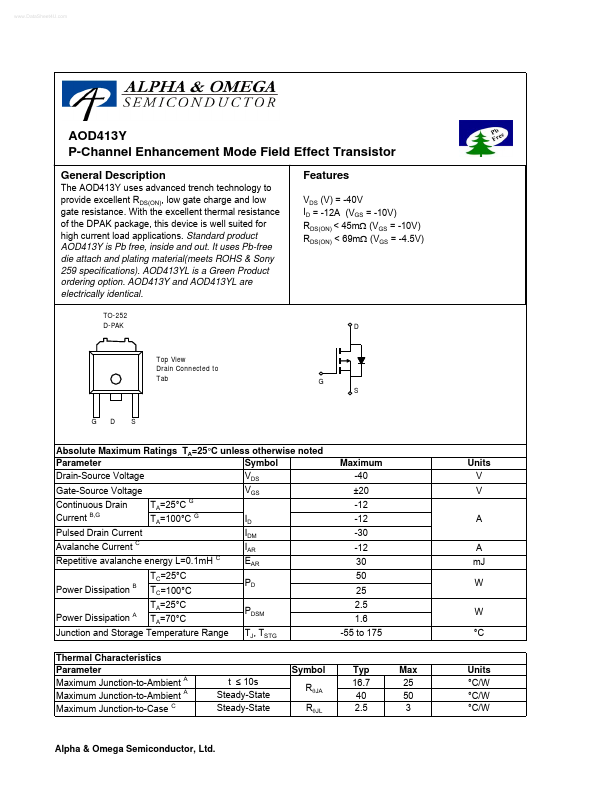
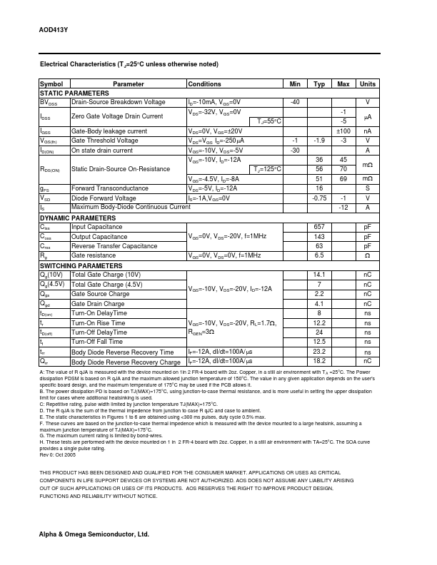
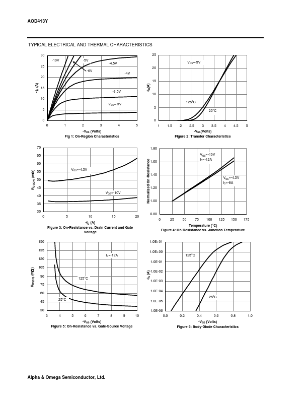
The AOD413Y uses advanced trench technology to provide excellent RDS(ON), low gate charge and low gate resistance.
With the excellent thermal resistance of the DPAK package, this device is well suited for high current load applications.
Standard product AOD413Y is Pb free, inside and out.
| Part number | AOD413Y |
|---|---|
| Manufacturer | Alpha & Omega Semiconductors |
| File Size | 142.88 KB |
| Description | P-Channel MOSFET |
| Datasheet |
AOD413Y Datasheet
|
|
|
|
| Part Number | Description | Manufacturer |
|---|---|---|
| AOD4130 | N-Channel MOSFET | INCHANGE |
| AOD4132 | N-Channel MOSFET | INCHANGE |
| AOD4136 | N-Channel MOSFET | INCHANGE |
| AOD413A | N-Channel MOSFET | INCHANGE |
| AOD4102 | N-Channel MOSFET | INCHANGE |
| Part Number | Description |
|---|---|
| AOD413 | P-Channel MOSFET |
| AOD4130 | 60V N-Channel MOSFET |
| AOD4132 | 30v N-Channel MOSFET |
| AOD4136 | POWER Transistor |
| AOD413A | 40V P-Channel MOSFET |
The following content is an automatically extracted verbatim text from the original manufacturer datasheet and is provided for reference purposes only.