Datasheet Details
| Part number | AOD603A |
|---|---|
| Manufacturer | Alpha & Omega Semiconductors |
| File Size | 767.47 KB |
| Description | 60V Complementary MOSFET |
| Download | AOD603A Download (PDF) |
|
|
| Part number | AOD603A |
|---|---|
| Manufacturer | Alpha & Omega Semiconductors |
| File Size | 767.47 KB |
| Description | 60V Complementary MOSFET |
| Download | AOD603A Download (PDF) |
|
|
|
The AOD603A uses advanced trench technology MOSFETs to provide excellent RDS(ON) and low gate charge.
The complementary MOSFETs may be used in H-bridge, Inverters and other applications.
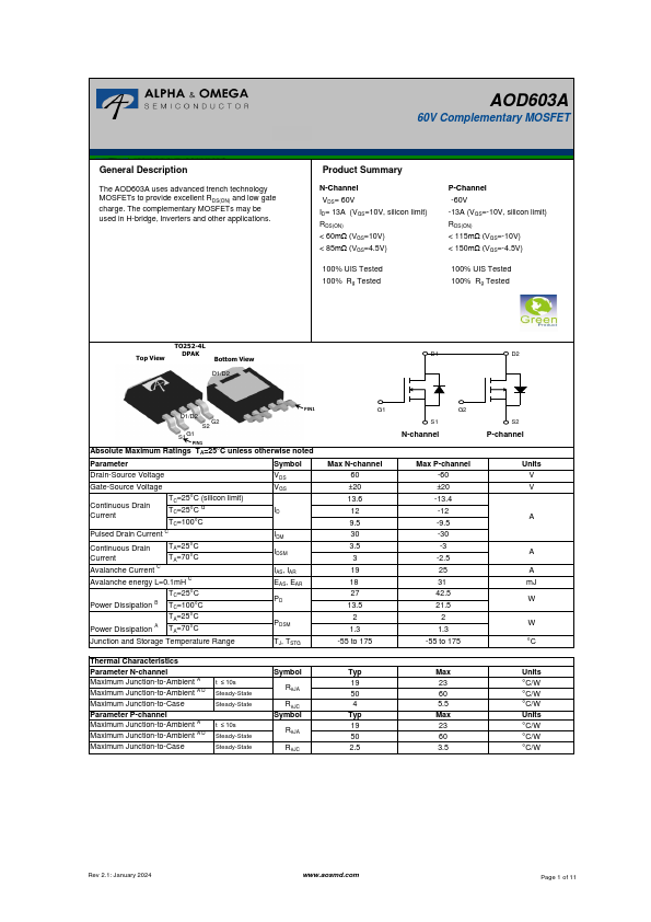
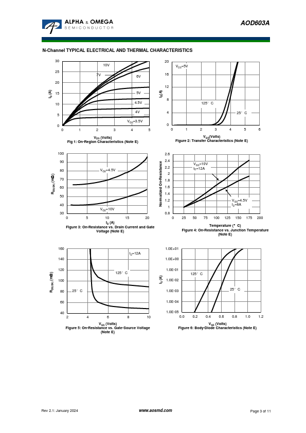
Product Summary N-Channel VDS= 60V ID= 13A (VGS=10V, silicon limit) RDS(ON) < 60mΩ (VGS=10V) < 85mΩ (VGS=4.5V) 100% UIS Tested 100% Rg Tested P-Channel -60V -13A (VGS=-10V, silicon limit) RDS(ON) < 115mΩ (VGS=-10V) < 150mΩ (VGS=-4.5V) 100% UIS Tested 100% Rg Tested Top View TO252-4L DPAK Bottom View D1/D2 D1 D2 PIN1 D1/D2 S2 G2 S1 G1 PIN1 Absolute Maximum Ratings TA=25°C unless otherwise noted Parameter Symbol Drain-Source Voltage VDS Gate-Source Voltage Continuous Drain Current TC=25°C (silicon limit) TC=25°C G TC=100°C Pulsed Drain Current C Continuous Drain Current Avalanche Current C TA=25°C TA=70°C Avalanche energy L=0.1mH C TC=25°C Power Dissipation B TC=100°C VGS ID IDM IDSM IAS, IAR EAS, EAR PD TA=25°C Power Dissipation A TA=70°C PDSM Junction and Storage Temperature Range TJ, TSTG G1 Max N-channel 60 ±20 13.6 12 9.5 30 3.5 3 19 18 27 13.5 2 1.3 -55 to 175 Thermal Characteristics Parameter N-channel Symbol Typ Maximum Junction-to-Ambient A t ≤ 10s Maximum Junction-to-Ambient A D Steady-State RqJA 19 50 Maximum Junction-to-Case Steady-State RqJC 4 Parameter P-channel Symbol Typ Maximum Junction-to-Ambient A t ≤ 10s Maximum Junction-to-Ambient A D Steady-State RqJA 19 50 Maximum Junction-to-Case Steady-State RqJC 2.5 G2 S1 N-channel Max P-channel -60 ±20 -13.4 -12 -9.5 -30 -3 -2.5 25 31 42.5 21.5 2 1.3 -55 to 175 Max 23 60 5.5 Max 23 60 3.5 S2 P-channel Units V V A A A mJ W W °C Units °C/W °C/W °C/W Units °C/W °C/W °C/W Rev 2.1: January 2024 www.aosmd.com Page 1 of 11 AOD603A N-Channel Electrical Characteristics (TJ=25°C unless otherwise noted) Symbol Parameter Conditions Min Typ Max Units STATIC PARAMETERS BVDSS Drain-Source Breakdown Voltage ID=250mA, VGS=0V 6
AOD603A 60V Complementary MOSFET General.
| Brand Logo | Part Number | Description | Manufacturer |
|---|---|---|---|
| AOD603A | Dual-Channel MOSFET | VBsemi |
| Part Number | Description |
|---|---|
| AOD603 | MOSFET |
| AOD600A70 | 700V N-Channel Power Transistor |
| AOD600A70P | N-Channel Power Transistor |
| AOD600A70R | N-Channel Power Transistor |
| AOD604 | MOSFET |
| AOD606 | MOSFET |
| AOD607 | MOSFET |
| AOD607A | 30V Complementary MOSFET |
| AOD609 | 40V Complementary MOSFET |
| AOD609G | Complementary Enhancement Mode Field Effect Transistor |