AOTF12N30
AOTF12N30 is N-Channel MOSFET manufactured by Alpha & Omega Semiconductors.
- Part of the AOT12N30 comparator family.
- Part of the AOT12N30 comparator family.
Description
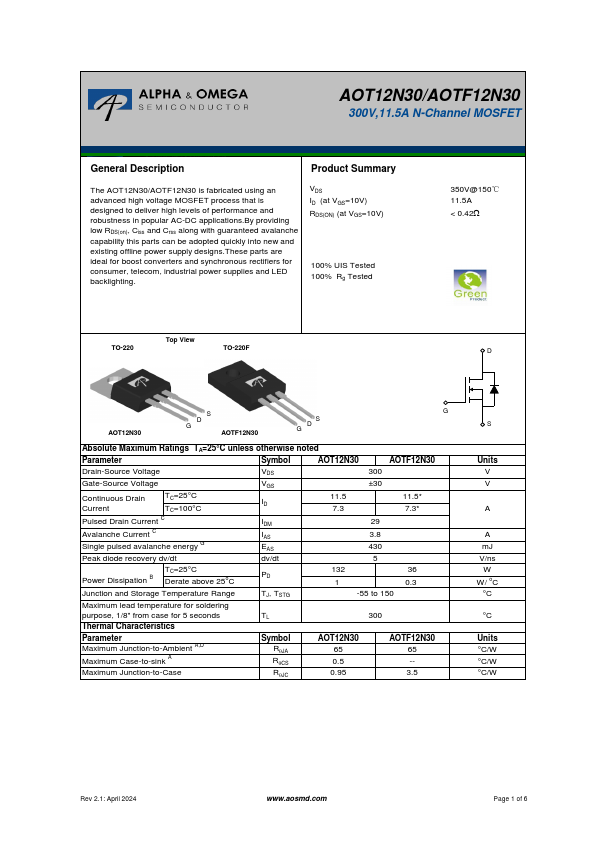
Product Summary
The AOT12N30/AOTF12N30 is fabricated using an advanced high voltage MOSFET process that is designed to deliver high levels of performance and robustness in popular AC-DC applications.By providing low RDS(on), Ciss and Crss along with guaranteed avalanche capability this parts can be adopted quickly into new and existing offline power supply designs.These parts are ideal for boost converters and synchronous rectifiers for consumer, tele, industrial power supplies and LED backlighting.
VDS ID (at VGS=10V) RDS(ON) (at VGS=10V)
100% UIS Tested 100% Rg Tested
350V@150℃ 11.5A < 0.42W
Top View
TO-220
TO-220F
AOT12N30
Absolute Maximum Ratings TA=25°C unless otherwise noted
Parameter
Symbol
AOT12N30
Drain-Source Voltage
Gate-Source Voltage
±30
Continuous Drain
TC=25°C
Current
TC=100°C
Pulsed Drain Current C
Avalanche Current C
Single pulsed avalanche energy G
Peak diode recovery dv/dt
IDM IAS EAS dv/dt
11.5-
7.3-
430 5
TC=25°C Power Dissipation B Derate above 25o...