AO4422A
Description
The AO4422A uses advanced trench technology to provide excellent RDS(ON) and low gate charge. This .. device is suitable for use as a load switch or in PWM applications. The source leads are separated to allow a Kelvin connection to the source, which may be used to bypass the source inductance. Standard Product AO4422A is Pb-free (meets ROHS & Sony 259 specifications). AO4422AL is a Green Product ordering option. AO4422A and AO4422AL are electrically identical.
Features
VDS (V) = 30V ID = 11A (V GS = 10V) RDS(ON) < 15mΩ (VGS = 10V) RDS(ON) < 24mΩ (VGS = 4.5V)
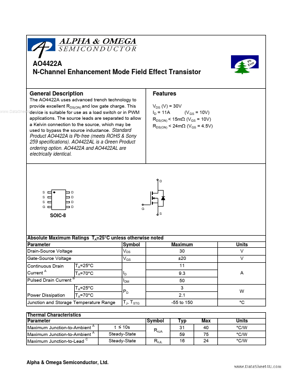
D S S S G D D D D
SOIC-8
Absolute Maximum Ratings TA=25°C unless otherwise noted Parameter Symbol VDS Drain-Source Voltage VGS Gate-Source Voltage Continuous Drain Current A Pulsed Drain Current Power Dissipation
Maximum 30 ±20 11 9.3 50 3 2.1 -55 to 150
Units V V A
TA=25°C TA=70°C TA=25°C TA=70°C ID IDM PD TJ, TSTG
W °C
Junction and Storage Temperature Range Thermal Characteristics Parameter Maximum...