ADL8100
ADL8100 is Low Noise Amplifier manufactured by Analog Devices.
FEATURES
- Low noise figure: 2.5 d B typical at 6 GHz to 14 GHz
- Single positive supply (self biased)
- High gain: 20 d B typical from 0.01 GHz to 6 GHz
- High OIP3: 38 d Bm typical from 0.01 GHz to 6 GHz
- Ro HS-pliant, 2 mm × 2 mm, 8-lead LFCSP
APPLICATIONS
- Satellite munication
- Telemunications
- Civilian radars
- Military radars
- Weather radars
- Electronic warfare
GENERAL DESCRIPTION
The ADL8100 is a gallium arsenide (Ga As), monolithic microwave integrated circuit (MMIC), pseudomorphic high electron mobility transistor (p HEMT), wideband low noise amplifier (LNA) that operates from 0.01 GHz to 20 GHz. The ADL8100 provides a typical gain of 20 d B at 0.01 GHz to 6 GHz, a 2.5 d B typical noise figure at 6 GHz to 14 GHz, and a typical output third-order intercept (OIP3) of 38 d Bm at 0.01 GHz to 6 GHz, requiring only 220 m A from a 5 V supply voltage. The power dissipation can be lowered at the expense of OIP3 and output power. The ADL8100 also features inputs and outputs that are DC-coupled and internally matched to 50 Ω.
The ADL8100 is housed in a Ro HS-pliant, 2 mm × 2 mm, 8-lead LFCSP.
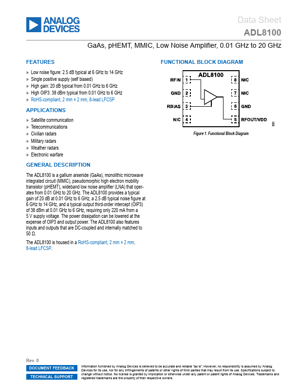
FUNCTIONAL BLOCK DIAGRAM
Figure 1. Functional Block Diagram
Rev. 0 DOCUMENT FEEDBACK TECHNICAL SUPPORT
Information furnished by Analog Devices is believed to be accurate and reliable "as is". However, no responsibility is assumed by Analog Devices for its use, nor for any infringements of patents or other rights of third parties that may result from its use. Specifications subject to change without notice. No license is granted by implication or otherwise under any patent or patent rights of Analog Devices. Trademarks and registered trademarks are the property of their respective owners.
Data Sheet
TABLE OF CONTENTS
Features
1 Applications 1 General Description
1 Functional Block Diagram...