ADL8102
ADL8102 is Low Noise Amplifier manufactured by Analog Devices.
FEATURES
- Single positive supply (self biased)
- Gain: 27 d B typical at 9 GHz to 19 GHz
- OP1d B: 13.5 d B typical at 1 GHz to 9 GHz
- OIP3: 25 d Bm typical at 1 GHz to 9 GHz
- Noise figure: 2.5 d B typical at 9 GHz to 19 GHz
- Ro HS-pliant, 3 mm × 3 mm, 16-lead LFCSP
APPLICATIONS
- Telemunications
- Satellite munications
- Military radar
- Weather radar
- Civil radar
- Electronic warfare
GENERAL DESCRIPTION
The ADL8102 is a gallium arsenide (Ga As), monolithic microwave integrated circuit (MMIC), pseudomorphic high electron mobility transistor (p HEMT), low noise wideband amplifier that operates from 1 GHz to 22 GHz.
The ADL8102 provides a typical gain of 27 d B at 9 GHz to 19 GHz, a 2.5 d B typical noise figure from 9 GHz to 19 GHz, a typical output third-order intercept (OIP3) of 25 d Bm at 1 GHz to 9 GHz, and a saturated output power (PSAT) of up to 15.5 d Bm, which requires
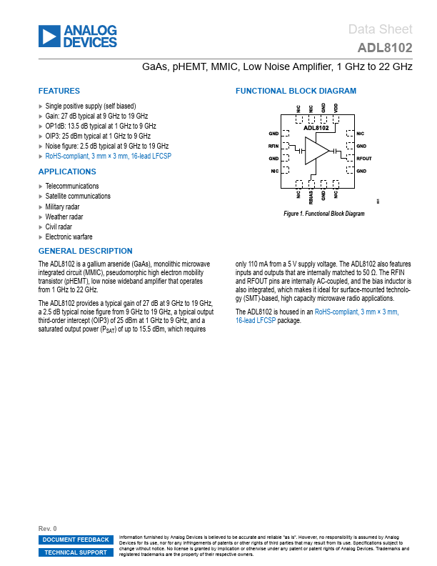
FUNCTIONAL BLOCK DIAGRAM
Figure 1. Functional Block Diagram only 110 m A from a 5 V supply voltage. The ADL8102 also features inputs and outputs that are internally matched to 50 Ω. The RFIN and RFOUT pins are internally AC-coupled, and the bias inductor is also integrated, which makes it ideal for surface-mounted technology (SMT)-based, high capacity microwave radio applications. The ADL8102 is housed in an Ro HS-pliant, 3 mm × 3 mm, 16-lead LFCSP package.
Rev. 0 DOCUMENT FEEDBACK TECHNICAL SUPPORT
Information furnished by Analog Devices is believed to be accurate and reliable "as is". However, no responsibility is assumed by Analog Devices for its use, nor for any infringements of patents or other rights of third parties that may result from its use. Specifications subject to change without notice. No license is granted by implication or otherwise under any patent or patent rights of Analog Devices. Trademarks and registered trademarks are the property of their respective owners.
Data Sheet
TABLE OF CONTENTS
Features
1 Applications......