Datasheet4U Logo Datasheet4U.com

ADN2890 Datasheet - Analog Devices

Limiting Amplifier

ADN2890 Features

* SFP reference design available Input sensitivity: 3 mV p-p 80 ps rise/fall times CML outputs: 700 mV p-p differential Programmable LOS detector: 2 mV to 13 mV Rx signal strength indicator (RSSI): SFF-8472 compliant average power measurement Single-supply operation: 3.3 V Low power dissipation: 130 m

ADN2890 General Description

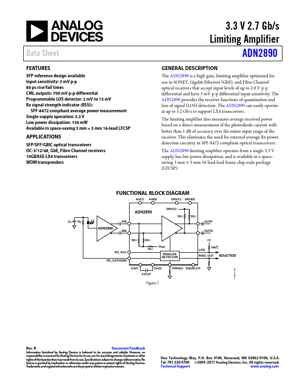
The ADN2890 is a high gain, limiting amplifier optimized for use in SONET, Gigabit Ethernet (GbE), and Fibre Channel optical receivers that accept input levels of up to 2.0 V p-p differential and have 3 mV p-p differential input sensitivity. The ADN2890 provides the receiver functions of quantizatio.

ADN2890 Datasheet (349.66 KB)

Preview of ADN2890 PDF

Datasheet Details

Part number:

ADN2890

Manufacturer:

Analog Devices ↗

File Size:

349.66 KB

Description:

Limiting amplifier.

📁 Related Datasheet

ADN2891 Amplifier (Analog Devices)

ADN2892 Limiting Amplifier (Analog Devices)

ADN2804 Clock and Data Recovery (Analog Devices)

ADN2805 1.25 Gbps Clock and Data Recovery IC (Analog Devices)

ADN2806 Clock and Data Recovery IC (Analog Devices)

ADN2807 Clock and Data Recovery (Analog Devices)

ADN2809 Multi-Rate to 2.7Gbps Clock and Data Recovery IC with Limiting Amplifier (Analog Devices)

ADN2811 OC-48/OC-48 FEC Clock and Data Recovery IC (Analog Devices)

ADN2812 Continuous Rate 12.3 Mb/s to 2.7 Gb/s Clock and Data Recovery IC with Integrated Limiting Amp (Analog Devices)

ADN2813 Clock and Data Recovery IC (Analog Devices)

TAGS

ADN2890 Limiting Amplifier Analog Devices

Image Gallery

ADN2890 Datasheet Preview Page 2 ADN2890 Datasheet Preview Page 3

ADN2890 Distributor