ADPA1107
ADPA1107 is GaN Power Amplifier manufactured by Analog Devices.
FEATURES
POUT with PIN = 27.0 d Bm: 45.0 d Bm typical at 5.4 GHz to 6.0 GHz Small signal gain: 30.5 d B typical at 4.8 GHz to 5.4 GHz Frequency range: 4.8 GHz to 6.0 GHz PAE with PIN = 27.0 d Bm: 56.5% typical at 5.4 GHz to 6.0 GHz VDD: 28 V at IDQ = 350 m A with a 10% duty cycle 40-lead, 6 mm × 6 mm, LFCSP
APPLICATIONS
Weather radars Marine radars Military radars
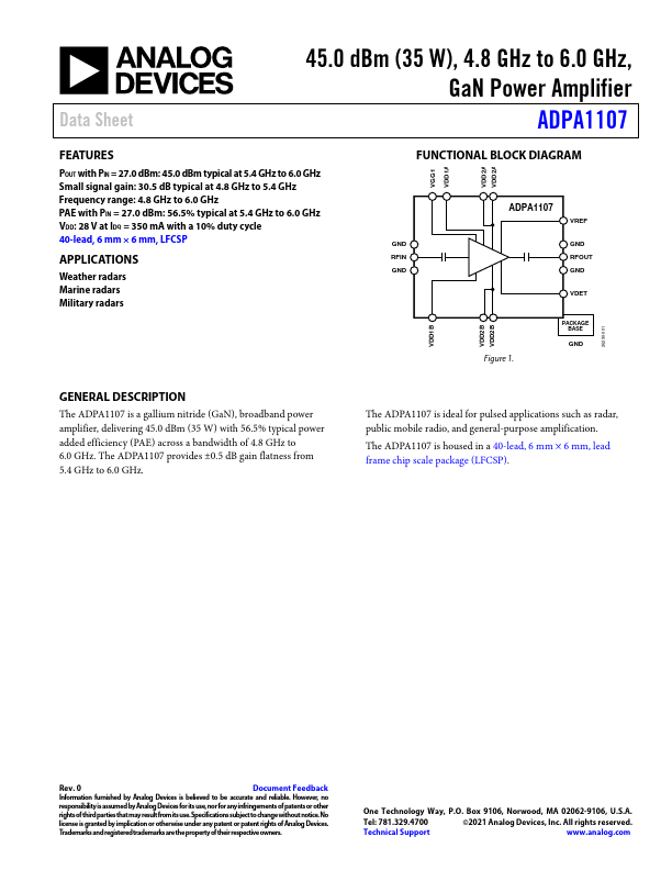
FUNCTIONAL BLOCK DIAGRAM
VGG1 VDD1A VDD2A VDD2A
GND RFIN GND
VREF
GND RFOUT GND
VDET
Figure 1.
PACKAGE BASE
VDD1B VDD2B VDD2B
26290-001
GENERAL DESCRIPTION
The ADPA1107 is a gallium nitride (Ga N), broadband power amplifier, delivering 45.0 d Bm (35 W) with 56.5% typical power added efficiency (PAE) across a bandwidth of 4.8 GHz to 6.0 GHz. The ADPA1107 provides ±0.5 d B gain flatness from 5.4 GHz to 6.0 GHz.
The ADPA1107 is ideal for pulsed applications such as radar, public mobile radio, and general-purpose amplification.
The ADPA1107 is housed in a 40-lead, 6 mm × 6 mm, lead frame chip scale package (LFCSP).
Rev. 0
Document Feedback
Information furnished by Analog Devices is believed to be accurate and reliable. However, no responsibility is assumed by Analog Devices for its use, nor for any infringements of patents or other rights of third parties that may result from its use. Specifications subject to change without notice. No license is granted by implication or otherwise under any patent or patent rights of Analog Devices.
Trademarks and registered trademarks are the property of their respective owners.
One Technology Way, P.O. Box 9106, Norwood, MA 02062-9106, U.S.A.
Tel: 781.329.4700
©2021 Analog Devices, Inc. All rights reserved.
Technical Support
.analog.
TABLE OF CONTENTS
Features
1 Applications 1 Functional Block Diagram...