Datasheet Summary
..
Preliminary Technical Data
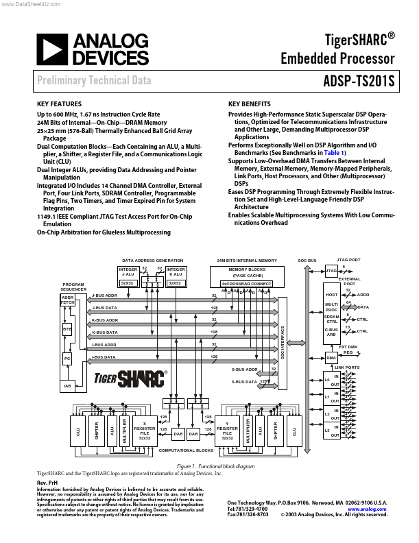
KEY Features
Up to 600 MHz, 1.67 ns Instruction Cycle Rate 24M Bits of Internal- On-Chip- DRAM Memory 25×25 mm (576-Ball) Thermally Enhanced Ball Grid Array Package Dual putation Blocks- Each Containing an ALU, a Multiplier, a Shifter, a Register File, and a munications Logic Unit (CLU) Dual Integer ALUs, providing Data Addressing and Pointer Manipulation Integrated I/O Includes 14 Channel DMA Controller, External Port, Four Link Ports, SDRAM Controller, Programmable Flag Pins, Two Timers, and Timer Expired Pin for System Integration 1149.1 IEEE pliant JTAG Test Access Port for On-Chip Emulation On-Chip Arbitration for Glueless...