CP753V Description
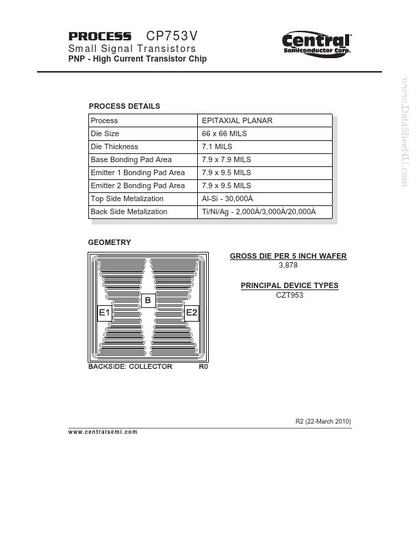
PROCESS Small Signal Transistors CP753V PNP - High Current Transistor Chip .. c o m PROCESS CP753V Typical R2 (22-March 2010) w w.
CP753V Key Features
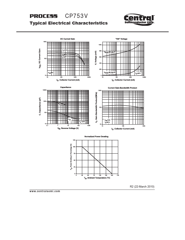
- s e m i . c o m PROCESS CP753V Typical
CP753V is PNP Transistor manufactured by Central Semiconductor.
| Part Number | Description |
|---|---|
| CP757X | P-Channel MOSFET |
| CP759R | Small Signal MOSFET Transistor |
| CP704 | PNP Transistor |
| CP705 | PNP Transistor |
| CP707 | PNP Transistor |
PROCESS Small Signal Transistors CP753V PNP - High Current Transistor Chip .. c o m PROCESS CP753V Typical R2 (22-March 2010) w w.