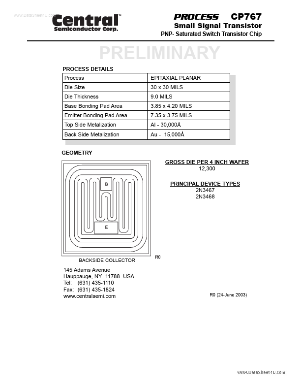
The following content is an automatically extracted verbatim text
from the original manufacturer datasheet and is provided for reference purposes only.
View original datasheet text
www.DataSheet4U.com
PROCESS
Small Signal Transistor
CP767
PNP- Saturated Switch Transistor Chip
PRELIMINARY
PROCESS DETAILS Process Die Size Die Thickness Base Bonding Pad Area Emitter Bonding Pad Area Top Side Metalization Back Side Metalization GEOMETRY GROSS DIE PER 4 INCH WAFER 12,300 PRINCIPAL DEVICE TYPES 2N3467 2N3468 EPITAXIAL PLANAR 30 x 30 MILS 9.0 MILS 3.85 x 4.20 MILS 7.35 x 3.75 MILS Al - 30,000Å Au - 15,000Å
BACKSIDE COLLECTOR
145 Adams Avenue Hauppauge, NY 11788 USA Tel: (631) 435-1110 Fax: (631) 435-1824 www.centralsemi.