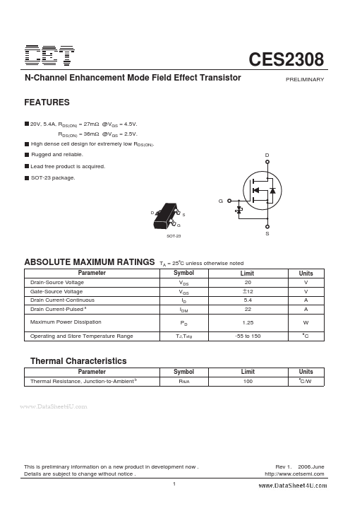
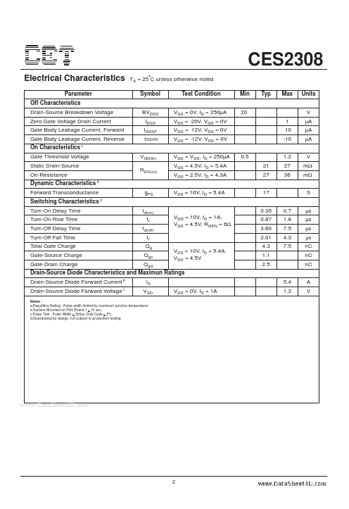
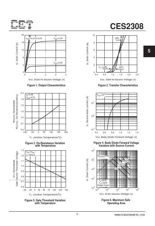
CES2308 Description
CES2308 N-Channel Enhancement Mode Field Effect Transistor.
| Part number | CES2308 |
|---|---|
| Download | CES2308 Datasheet (PDF) |
| File Size | 179.16 KB |
| Manufacturer | Chino-Excel Technology |
| Description | N-Channel MOSFET |
|
|
| Part Number | Description |
|---|---|
| CES2302 | N-Channel MOSFET |
| CES2303 | P-Channel MOSFET |
| CES2305 | P-Channel MOSFET |
| CES2307 | P-Channel MOSFET |
| CES2309 | P-Channel MOSFET |
CES2308 N-Channel Enhancement Mode Field Effect Transistor.