CY14B512I Description
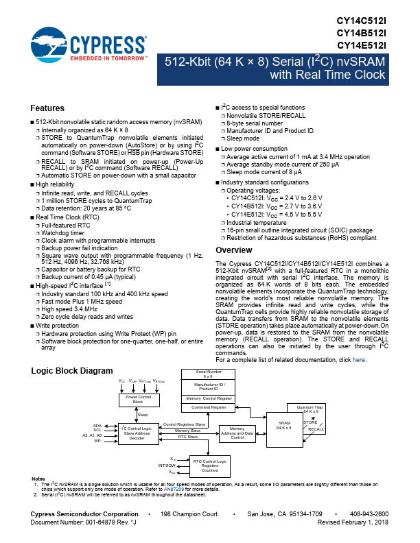
512-Kbit (64 K × 8) Serial (I C) nvSRAM with Real Time Clock 512-Kbit (64 K × 8) Serial (I2C) nvSRAM with Real Time Clock CY14C512I CY14B512I, CY14E512I.
CY14B512I Key Features
- 512-Kbit nonvolatile static random access memory (nvSRAM)
- Internally organized as 64 K × 8
- STORE to QuantumTrap nonvolatile elements initiated automatically on power-down (AutoStore) or by using I2C mand (Softwa
- RECALL to SRAM initiated on power-up (Power-Up RECALL) or by I2C mand (Software RECALL)
- Automatic STORE on power-down with a small capacitor
- High reliability
- Infinite read, write, and RECALL cycles
- 1 million STORE cycles to QuantumTrap
- Data retention: 20 years at 85 C
- Real Time Clock (RTC)