CY2291
Three-PLL General Purpose EPROM
Programmable Clock Generator
Features
■ Three integrated phase-locked loops
■ EPROM programmability
■ Factory-programmable (CY2291) or field-programmable
(CY2291F) device options
■ Low-skew, low-jitter, high-accuracy outputs
■ Power-management options (Shutdown, OE, Suspend)
■ Frequency select option
■ Smooth slewing on CPUCLK
■ Configurable 3.3 V or 5 V operation
■ 20-pin SOIC Package
Functional Description
The CY2291 is a third-generation family of clock generators. The
CY2291 is upwardly compatible with the industry standard
ICD2023 and ICD2028 and continues their tradition by providing
a high level of customizable features to meet the diverse clock
synchoronous systems.
All parts provide a highly configurable set of close for PC
motherboard applications. Each of four configurable clock
outputs (CLKA-CLKD) can be assigned 1 of 30 frequencies in
any combination. Multiple outputs configured for the same or
related[3] frequencies have low (<500 ps) skew, in effect
providing on-chip buffering for heavily loaded signals.
The CY2291 can be configured for either 5 V or 3.3 V operation.
The internal ROM tables use EPROM technology, allowing full
customization of output frequencies. The reference oscillator has
been designed for 10 MHz to 25 MHz crystals, providing
additional flexibility. No external components are required with
this crystal. Alternatively, an external reference clock of
frequency between 1 MHZ to 30 MHz can be used. Customers
using the 32 kHz oscillator must connect a 10-MW resistor in
parallel with the 32 kHz crystal.
Part Number Outputs
Input Frequency Range
CY2291
8 10 MHz – 25 MHz (external crystal)
1 MHz – 30 MHz (reference clock)
CY2291I
8 10 MHz – 25 MHz (external crystal)
1 MHz – 30 MHz (reference clock)
CY2291F
8 10 MHz – 25 MHz (external crystal)
1 MHz – 30 MHz (reference clock)
CY2291FI
8 10 MHz – 25 MHz (external crystal)
1 MHz – 30 MHz (reference clock)
Output Frequency Range
76.923 kHz – 100 MHz (5 V)
76.923 kHz – 80 MHz (3.3 V)
76.923 kHz – 90 MHz (5 V)
76.923 kHz – 66.6 MHz (3.3 V)
76.923 kHz – 90 MHz (5 V)
76.923 kHz – 66.6 MHz (3.3 V)
76.923 kHz – 80 MHz (5 V)
76.923 kHz – 60.0 MHz (3.3 V)
Specifics
Factory programmable
Commercial temperature
Factory programmable
Industrial temperature
Field programmable
Commercial temperature
Field programmable
Industrial temperature
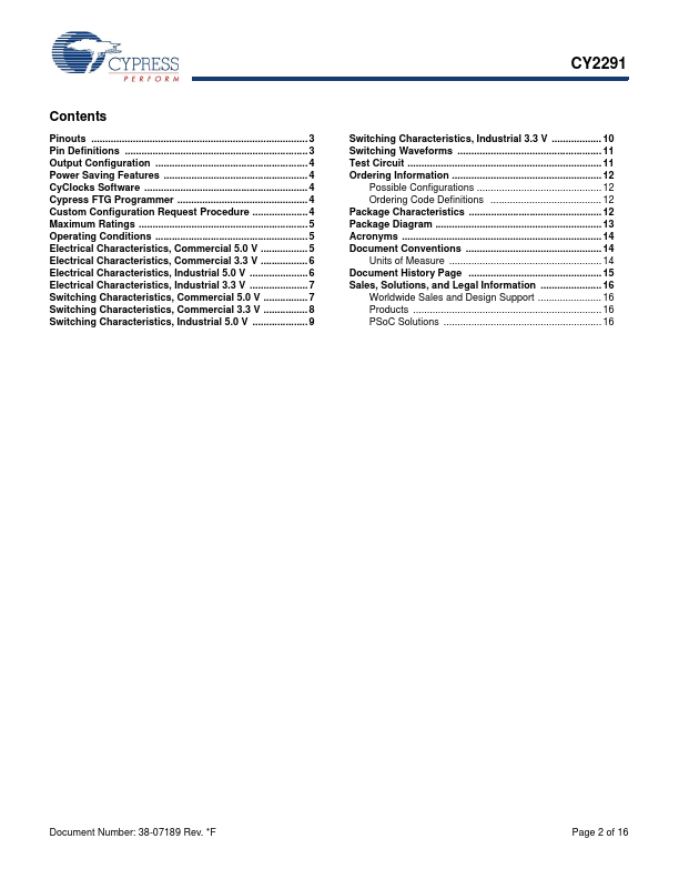
Logic Block Diagram
32XIN
32XOUT
XTALIN
XTALOUT
S0
S1
S2/SUSPEND
OSC.
OSC.
CPLL
(8 BIT)
UPLL
(10 BIT)
SPLL
(8 BIT)
/1,2,4
/1,2,4,8
/1,2,3,4,5,6
/8,10,12,13
/20,24,26,40
/48,52,96,104
/2,3,4
32K
XBUF
CPUCLK
CLKA
CLKB
CLKC
CLKD
CLKF
SHUTDOWN/
OE
CONFIG
EPROM
Cypress Semiconductor Corporation • 198 Champion Court
Document Number: 38-07189 Rev. *F
• San Jose, CA 95134-1709 • 408-943-2600
Revised December 1, 2011