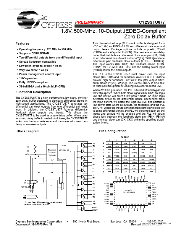
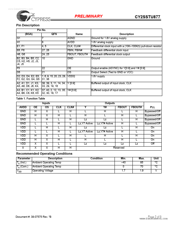
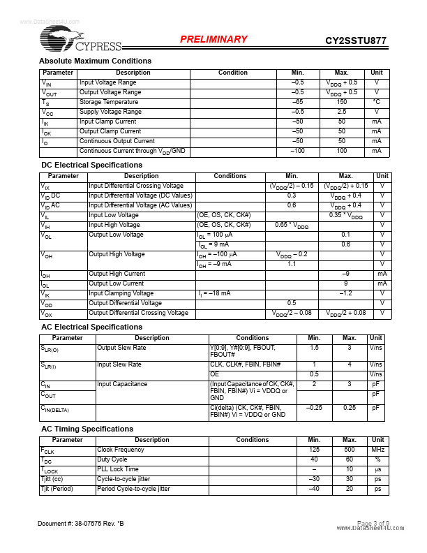
Datasheet4U Logo Datasheet4U.com

CY2SSTU877 - 10-Output JEDEC-Compliant Zero Delay Buffer

General Description

The CY2SSTU877 is a high-performance, low-skew, low-jitter zero delay buffer designed to distribute differential clocks in high-speed applications.

The CY2SSTU877 generates ten differential pair clock outputs from one differential pair clock input.

Key Features

  • Operating frequency: 125 MHz to 500 MHz.
  • Supports DDRII SDRAM.
  • Ten differential outputs from one differential input.
  • Spread-Spectrum-compatible.
  • Low jitter (cycle-to-cycle): < 40 ps.
  • Very low skew: < 40 ps.
  • Power management control input.
  • 1.8V operation.
  • Fully JEDEC-compliant.
  • 52-ball BGA and a 40-pin MLF (QFN) This phase-locked loop (PLL) clock buffer is designed for a VDD of 1.8V, an AVDD of 1.8V and dif.

📥 Download Datasheet

Full PDF Text Transcription for CY2SSTU877 (Reference)

Note: Below is a high-fidelity text extraction (approx. 800 characters) for CY2SSTU877. For precise diagrams, and layout, please refer to the original PDF.

www.DataSheet4U.com PRELIMINARY CY2SSTU877 1.8V, 500-MHz, 10-Output JEDEC-Compliant Zero Delay Buffer Features • Operating frequency: 125 MHz to 500 MHz • Supports DDRII ...

View more extracted text
r Features • Operating frequency: 125 MHz to 500 MHz • Supports DDRII SDRAM • Ten differential outputs from one differential input • Spread-Spectrum-compatible • Low jitter (cycle-to-cycle): < 40 ps • Very low skew: < 40 ps • Power management control input • 1.8V operation • Fully JEDEC-compliant • 52-ball BGA and a 40-pin MLF (QFN) This phase-locked loop (PLL) clock buffer is designed for a VDD of 1.8V, an AVDD of 1.8V and differential data input and output levels. Package options include a plastic 52-ball VFBGA and a 40-pin MLF (QFN).