CY7C1021BV33
CY7C1021BV33 is 64K x 16 Static RAM manufactured by Cypress.
- Part of the CY7 comparator family.
- Part of the CY7 comparator family.
Features
- 3.3V operation (3.0V- 3.6V)
- High speed
- t AA = 10/12/15 ns
- CMOS for optimum speed/power
- Low Active Power (L version)
- 576 m W (max.)
- Low CMOS Standby Power (L version)
- 1.80 m W (max.)
- Automatic power-down when deselected
- Independent control of upper and lower bits
- Available in 44-pin TSOP II and 400-mil SOJ
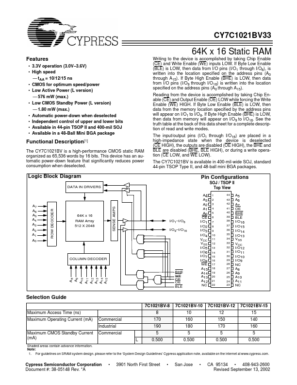
- Available in a 48-Ball Mini BGA package Writing to the device is acplished by taking Chip Enable (CE) and Write Enable (WE) inputs LOW. If Byte Low Enable (BLE) is LOW, then data from I/O pins (I/O1 through I/O8), is written into the location specified on the address pins (A0 through A15). If Byte High Enable (BHE) is LOW, then data from I/O pins (I/O9 through I/O16) is written into the location specified on the address pins (A0 through A15). Reading from the device is acplished by taking Chip Enable (CE) and Output Enable (OE) LOW while forcing the Write Enable (WE) HIGH. If Byte Low Enable (BLE) is LOW, then data from the memory location specified by the address pins will appear on I/O1 to I/O8. If Byte High Enable (BHE) is LOW, then data from memory will appear on I/O9 to I/O16. See the truth table at the back of this data sheet for a plete description of read and write modes. The input/output pins (I/O1 through I/O16) are placed in a high-impedance state when the device is deselected (CE HIGH), the outputs are disabled (OE HIGH), the BHE and BLE are disabled (BHE, BLE HIGH), or during a write operation (CE LOW, and WE LOW). The CY7C1021BV is available in 400-mil-wide SOJ, standard 44-pin TSOP Type II, and 48-ball mini BGA packages.
Functional Description
[1]
The CY7C1021BV is a high-performance CMOS static RAM organized as 65,536 words by 16 bits. This device has an automatic power-down feature that significantly reduces power consumption when deselected.
Logic Block Diagram
DATA IN DRIVERS
Pin Configurations
SOJ / TSOP II Top View A4 A3 A2 A1 A0 CE I/O1 I/O2 I/O3 I/O4 VCC VSS I/O5 I/O6 I/O7 I/O8 WE A15 A14 A13 A12 NC
1 2 3 4 5 6...