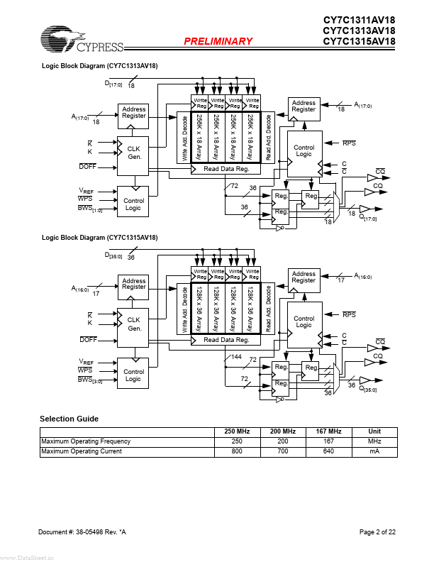
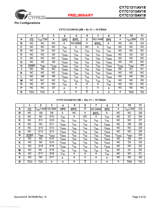
CY7C1313AV18 Description
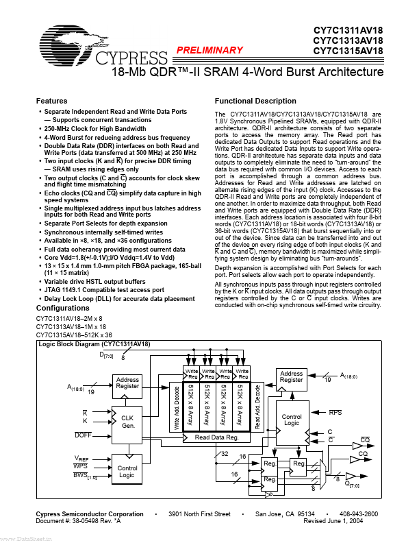
The CY7C1311AV18/CY7C1313AV18/CY7C1315AV18 are 1.8V Synchronous Pipelined SRAMs, equipped with QDR-II architecture. QDR-II architecture consists of two separate ports to access the memory array. The Read port has dedicated Data Outputs to support Read operations and the Write Port has dedicated Data Inputs to support Write operations.
CY7C1313AV18 Key Features
- Separate Independent Read and Write Data Ports
- Supports concurrent transactions
- 250-MHz Clock for High Bandwidth
- 4-Word Burst for reducing address bus frequency
- Double Data Rate (DDR) interfaces on both Read and Write Ports (data transferred at 500 MHz) at 250 MHz
- Two input clocks (K and K) for precise DDR timing
- SRAM uses rising edges only
- Two output clocks (C and C) accounts for clock skew and flight time mismatching
- Echo clocks (CQ and CQ) simplify data capture in high speed systems
- Single multiplexed address input bus latches address inputs for both Read and Write ports