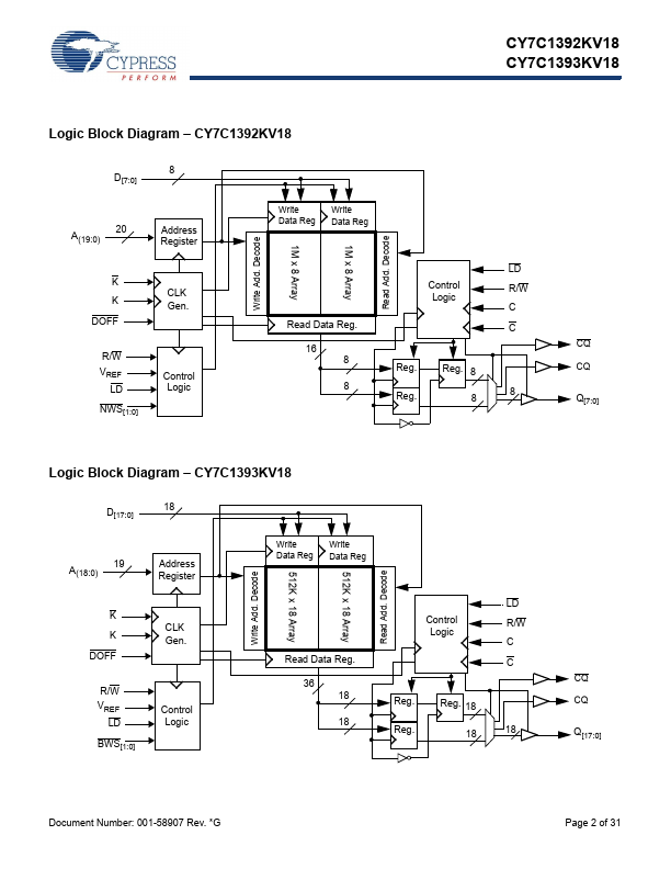
Datasheet4U Logo Datasheet4U.com

CY7C1393KV18 - 18-Mbit DDR II SIO SRAM Two-Word Burst Architecture

Download the CY7C1393KV18 datasheet PDF (CY7C1392KV18 included). The manufacturer datasheet provides complete specifications, pinout details, electrical characteristics, and typical applications for 18-mbit ddr ii sio sram two-word burst architecture.

Features

  • 18-Mbit density (2M × 8, 1M × 18).
  • 333-MHz clock for high bandwidth.
  • Two-word burst for reducing address bus frequency.
  • Double data rate (DDR) interfaces (data transferred at 666 MHz) at 333 MHz.
  • Two input clocks (K and K) for precise DDR timing.
  • SRAM uses rising edges only.
  • Two input clocks for output data (C and C) to minimize clock skew and flight time mismatches.
  • Echo clocks (CQ and CQ) simplify data capture in high-speed systems.
  • Synchronous int.

📥 Download Datasheet

Note: The manufacturer provides a single datasheet file (CY7C1392KV18-CypressSemiconductor.pdf) that lists specifications for multiple related part numbers.
Other Datasheets by Cypress Semiconductor

Full PDF Text Transcription

Click to expand full text
CY7C1392KV18 CY7C1393KV18 18-Mbit DDR II SIO SRAM Two-Word Burst Architecture 18-Mbit DDR II SIO SRAM Two-Word Burst Architecture Features ■ 18-Mbit density (2M × 8, 1M × 18) ■ 333-MHz clock for high bandwidth ■ Two-word burst for reducing address bus frequency ■ Double data rate (DDR) interfaces (data transferred at 666 MHz) at 333 MHz ■ Two input clocks (K and K) for precise DDR timing ❐ SRAM uses rising edges only ■ Two input clocks for output data (C and C) to minimize clock skew and flight time mismatches ■ Echo clocks (CQ and CQ) simplify data capture in high-speed systems ■ Synchronous internally self timed writes ■ DDR II operates with 1.5 cycle read latency when DOFF is asserted HIGH ■ Operates similar to DDR I device with one cycle read latency when DOFF is asserted LOW ■ 1.
Published: |