Datasheet4U Logo Datasheet4U.com

CY7C1447AV33 - 36-Mbit Flow-Through SRAM

Download the CY7C1447AV33 datasheet PDF (CY7C1443AV33 included). The manufacturer datasheet provides complete specifications, pinout details, electrical characteristics, and typical applications for 36-mbit flow-through sram.

Description

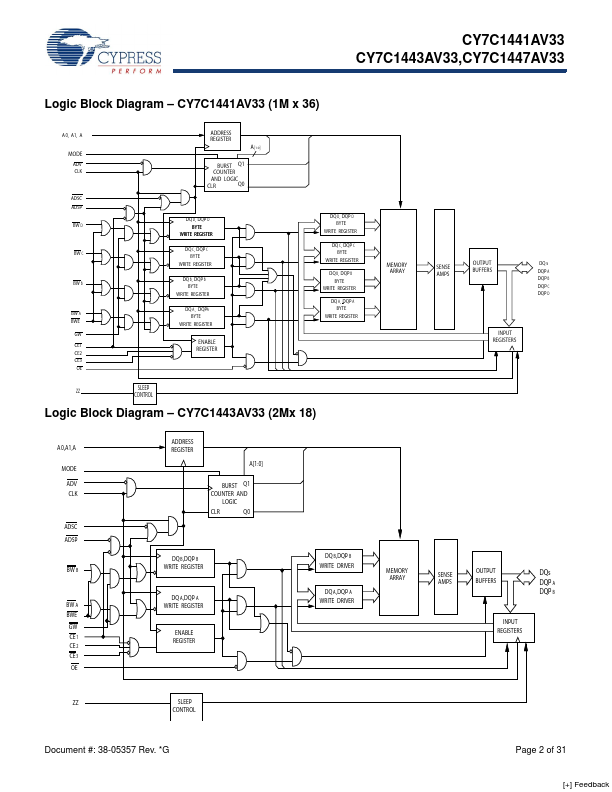
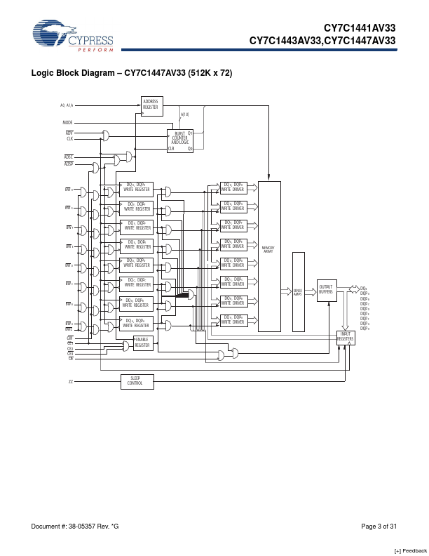
Maximum Access Time Maximum Operating Current Maximum CMOS Standby Current Functional Description The CY7C1441AV33/

Features

  • Supports 133-MHz bus operations.
  • 1M x 36/2M x 18/512K x 72 common IO.
  • 3.3V core power supply.
  • 2.5V or 3.3V IO power supply.
  • Fast clock-to-output times.
  • 6.5 ns (133-MHz version).
  • Provide high-performance 2-1-1-1 access rate.
  • User-selectable burst counter supporting Intel® Pentium® interleaved or linear burst sequences.
  • Separate processor and controller address strobes.
  • Synchronous self-timed write.
  • Asynchronous output enable.
  • CY7C1441AV.

📥 Download Datasheet

Note: The manufacturer provides a single datasheet file (CY7C1443AV33-CypressSemiconductor.pdf) that lists specifications for multiple related part numbers.
Other Datasheets by Cypress Semiconductor

Full PDF Text Transcription

Click to expand full text
CY7C1441AV33 CY7C1443AV33,CY7C1447AV33 36-Mbit (1M x 36/2M x 18/512K x 72) Flow-Through SRAM Features ■ Supports 133-MHz bus operations ■ 1M x 36/2M x 18/512K x 72 common IO ■ 3.3V core power supply ■ 2.5V or 3.3V IO power supply ■ Fast clock-to-output times ❐ 6.5 ns (133-MHz version) ■ Provide high-performance 2-1-1-1 access rate ■ User-selectable burst counter supporting Intel® Pentium® interleaved or linear burst sequences ■ Separate processor and controller address strobes ■ Synchronous self-timed write ■ Asynchronous output enable ■ CY7C1441AV33, CY7C1443AV33 available in JEDEC-standard Pb-free 100-pin TQFP package, Pb-free and non-lead-free 165-ball FBGA package. CY7C1447AV33 available in Pb-free and non-lead-free 209-ball FBGA package ■ IEEE 1149.
Published: |