Datasheet4U Logo Datasheet4U.com

CY7C2563KV18 - 72-Mbit QDR-II SRAM 4-Word Burst Architecture

Download the CY7C2563KV18 datasheet PDF. This datasheet also covers the CY7C2561KV18 variant, as both devices belong to the same 72-mbit qdr-ii sram 4-word burst architecture family and are provided as variant models within a single manufacturer datasheet.

General Description

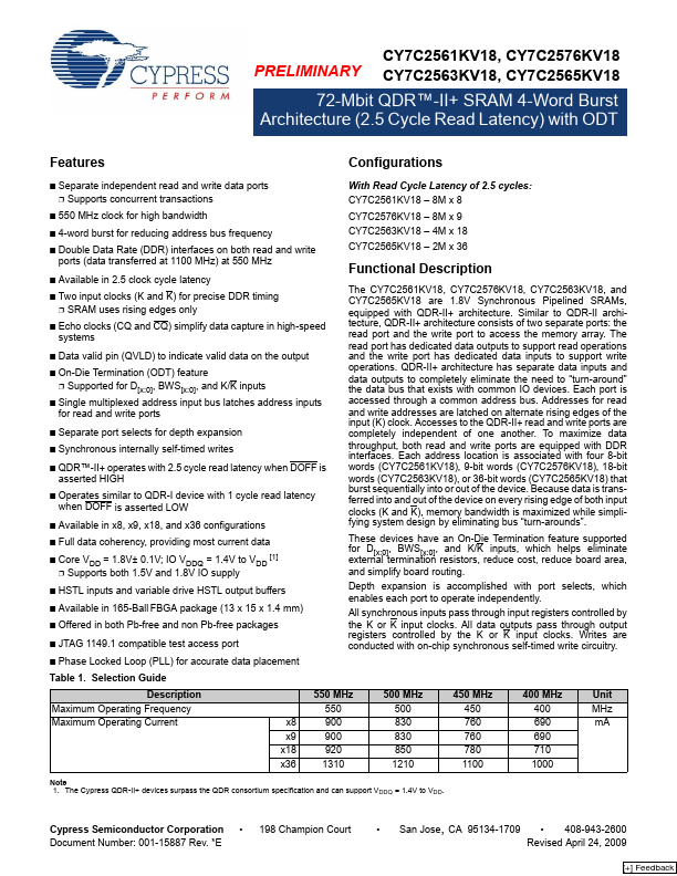
The CY7C2561KV18, CY7C2576KV18, CY7C2563KV18, and CY7C2565KV18 are 1.8V Synchronous Pipelined SRAMs, equipped with QDR-II+ architecture.

Similar to QDR-II architecture, QDR-II+ architecture consists of two separate ports: the read port and the write port to access the memory array.

Key Features

  • Configurations With Read Cycle Latency of 2.5 cycles: CY7C2561KV18.
  • 8M x 8 CY7C2576KV18.
  • 8M x 9 CY7C2563KV18.
  • 4M x 18 CY7C2565KV18.
  • 2M x 36 Separate independent read and write data ports.
  • Supports concurrent transactions 550 MHz clock for high bandwidth 4-word burst for reducing address bus frequency Double Data Rate (DDR) interfaces on both read and write ports (data transferred at 1100 MHz) at 550 MHz Available in 2.5 clock cycle latency Two inp.

📥 Download Datasheet

Note: The manufacturer provides a single datasheet file (CY7C2561KV18_CypressSemiconductor.pdf) that lists specifications for multiple related part numbers.

Full PDF Text Transcription for CY7C2563KV18 (Reference)

Note: Below is a high-fidelity text extraction (approx. 800 characters) for CY7C2563KV18. For precise diagrams, and layout, please refer to the original PDF.

www.DataSheet.co.kr PRELIMINARY CY7C2561KV18, CY7C2576KV18 CY7C2563KV18, CY7C2565KV18 72-Mbit QDR™-II+ SRAM 4-Word Burst Architecture (2.5 Cycle Read Latency) with ODT Fe...

View more extracted text
I+ SRAM 4-Word Burst Architecture (2.5 Cycle Read Latency) with ODT Features ■ Configurations With Read Cycle Latency of 2.5 cycles: CY7C2561KV18 – 8M x 8 CY7C2576KV18 – 8M x 9 CY7C2563KV18 – 4M x 18 CY7C2565KV18 – 2M x 36 Separate independent read and write data ports ❐ Supports concurrent transactions 550 MHz clock for high bandwidth 4-word burst for reducing address bus frequency Double Data Rate (DDR) interfaces on both read and write ports (data transferred at 1100 MHz) at 550 MHz Available in 2.