CY7C1354BV25
Key Features
- Supports 225-MHz bus operations with zero wait states - Available speed grades are 225, 200 and 166 MHz
- Internally self-timed output buffer control to eliminate the need to use asynchronous OE
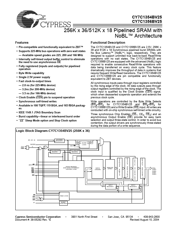
- Fully registered (inputs and outputs) for pipelined operation
- Single 2.5V power supply
- Fast clock-to-output times - 2.8 ns (for 225-MHz device) - 3.2ns (for 200-MHz device) - 3.5 ns (for 166-MHz device)
- Clock Enable (CEN) pin to suspend operation
- Synchronous self-timed writes
- Available in 100 TQFP, 119 BGA, and 165 fBGA packages
- IEEE 1149.1 JTAG Boundary Scan
- Burst capability-linear or interleaved burst order