CY7C1354D
Key Features
- Pin-compatible and functionally equivalent to ZBT
- Supports 200 MHz bus operations with zero wait states ❐ Available speed grade is 200 MHz
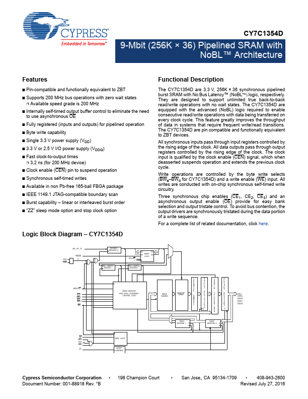
- Internally self-timed output buffer control to eliminate the need to use asynchronous OE
- Fully registered (inputs and outputs) for pipelined operation
- Single 3.3 V power supply (VDD)
- 3.3 V or 2.5 V I/O power supply (VDDQ)
- Fast clock-to-output times ❐ 3.2 ns (for 200 MHz device)
- Clock enable (CEN) pin to suspend operation
- Synchronous self-timed writes
- Available in non Pb-free 165-ball FBGA package