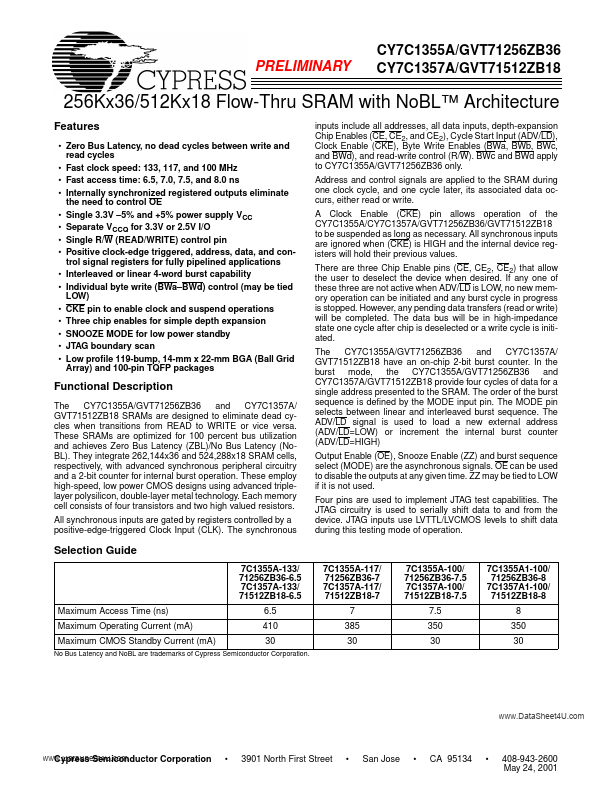
Datasheet4U Logo Datasheet4U.com

GVT7C1357A - 256K x 36 / 512K x 18 Flow Thru SRAM

This page provides the datasheet information for the GVT7C1357A, a member of the GVT71256ZB36 256K x 36 / 512K x 18 Flow Thru SRAM family.

Description

The CY7C1355A/GVT71256ZB36 and CY7C1357A/ GVT71512ZB18 SRAMs are designed to eliminate dead cycles when transitions from READ to WRITE or vice versa.

These SRAMs are optimized for 100 percent bus utilization and achieves Zero Bus Latency (ZBL)/No Bus Latency (NoBL).

Features

  • Zero Bus Latency, no dead cycles between write and read cycles.
  • Fast clock speed: 133, 117, and 100 MHz.
  • Fast access time: 6.5, 7.0, 7.5, and 8.0 ns.
  • Internally synchronized registered outputs eliminate the need to control OE.
  • Single 3.3V.
  • 5% and +5% power supply VCC.
  • Separate VCCQ for 3.3V or 2.5V I/O.
  • Single R/W (READ/WRITE) control pin.
  • Positive clock-edge triggered, address, data, and control signal registers fo.

📥 Download Datasheet

Datasheet preview – GVT7C1357A

Datasheet Details

Part number GVT7C1357A
Manufacturer Cypress Semiconductor
File Size 802.47 KB
Description 256K x 36 / 512K x 18 Flow Thru SRAM
Datasheet download datasheet GVT7C1357A Datasheet
Additional preview pages of the GVT7C1357A datasheet.
Other Datasheets by Cypress Semiconductor

Full PDF Text Transcription

Click to expand full text
( DataSheet : www.DataSheet4U.com ) 1CY7C1357A PRELIMINARY CY7C1355A/GVT71256ZB36 CY7C1357A/GVT71512ZB18 256Kx36/512Kx18 Flow-Thru SRAM with NoBL™ Architecture Features • Zero Bus Latency, no dead cycles between write and read cycles • Fast clock speed: 133, 117, and 100 MHz • Fast access time: 6.5, 7.0, 7.5, and 8.0 ns • Internally synchronized registered outputs eliminate the need to control OE • Single 3.3V –5% and +5% power supply VCC • Separate VCCQ for 3.3V or 2.
Published: |