Datasheet4U Logo Datasheet4U.com

MTA050P02DFJ6 - P-Channel Enhancement Mode MOSFET

Key Features

  • Low on-resistance.
  • Excellent thermal and electrical capabilities.
  • Pb-free lead plating and halogen-free package RDSON@VGS=-2.5V, ID=-3A RDSON@VGS=-1.8V, ID=-3A -20V -14.2A -5.2A 33.4mΩ(typ. ) 46.4mΩ(typ. ) 71.4mΩ(typ. ) Equivalent Circuit MTA050P02DFJ6 Outline DFNWB2×2-6L-J G:Gate S:Source D:Drain Ordering Information Device MTA050P02DFJ6-0-T1-G Package DFNWB2×2-6L-J (Pb-free lead plating and halogen-free package) Shipping 3000 pcs / tape & reel Environment fri.

📥 Download Datasheet

Datasheet Details

Part number MTA050P02DFJ6
Manufacturer Cystech Electonics
File Size 418.02 KB
Description P-Channel Enhancement Mode MOSFET
Datasheet download datasheet MTA050P02DFJ6 Datasheet

Full PDF Text Transcription (Reference)

The following content is an automatically extracted verbatim text from the original manufacturer datasheet and is provided for reference purposes only.

View original datasheet text
CYStech Electronics Corp. Spec. No. : C394DFJ6 Issued Date : 2015.09.03 Revised Date : Page No. : 1/9 -
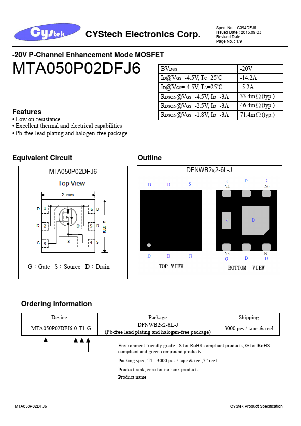
20V P-Channel Enhancement Mode MOSFET MTA050P02DFJ6 BVDSS ID@VGS=-4.5V, TC=25°C ID@VGS=-4.5V, TA=25°C RDSON@VGS=-4.5V, ID=-3A Features • Low on-resistance • Excellent thermal and electrical capabilities • Pb-free lead plating and halogen-free package RDSON@VGS=-2.5V, ID=-3A RDSON@VGS=-1.8V, ID=-3A -20V -14.2A -5.2A 33.4mΩ(typ.) 46.4mΩ(typ.) 71.4mΩ(typ.